
镓锌氧化物半导体薄膜的晶粒生长特性及其微结构研究
2016-04-21 12:37钟志有
中南民族大学学报(自然科学版) 2016年1期
钟志有, 陆 轴, 龙 路, 康 淮
(中南民族大学 电子信息工程学院, 智能无线通信湖北省重点实验室, 武汉 430074)
镓锌氧化物半导体薄膜的晶粒生长特性及其微结构研究
钟志有, 陆轴, 龙路, 康淮
(中南民族大学 电子信息工程学院, 智能无线通信湖北省重点实验室, 武汉 430074)
摘要采用ZnO:Ga3O2高密度陶瓷靶作为溅射源材料,利用射频磁控溅射技术在玻璃基片上制备了镓锌氧化物(GaZnO)半导体薄膜.基于X射线衍射仪的测试表征,研究了薄膜厚度对GaZnO样品晶粒生长特性和微结构性能的影响.研究结果表明:所制备的GaZnO样品为多晶薄膜,并且都具有六角纤锌矿型结构和(002)晶向的择优取向生长特性;其(002)取向程度、结晶性能和微结构参数等均与薄膜厚度密切相关.随着薄膜厚度的增大,GaZnO样品的(002)择优取向程度和晶粒尺寸表现为先增大后减小,而位错密度和晶格应变则表现为先减小后增大.当薄膜厚度为510 nm时,GaZnO样品具有最大的(002)晶向织构系数(2.959)、最大的晶粒尺寸(97.8 nm)、最小的位错密度(1.044×10(14) m(-2))和最小的晶格应变(5.887×10(-4)).
关键词磁控溅射;氧化锌薄膜;晶粒生长;微结构
Grain Growth and Microstructure of Gallium-Zinc Oxide Semiconductor Thin Films
ZhongZhiyou,LuZhou,LongLu,KangHuai
(Hubei Key Laboratory of Intelligent Wireless Communications, College of Electronic Information Engineering,South-Central University for Nationalities, Wuhan 430074, China)
AbstractThe gallium-zinc oxide (GaZnO) semiconductor thin films were deposited on glass substrates by radio-frequency magnetron sputtering technique using the ceramic target fabricated by sintering the mixture of ZnO and Ga2O3nanometer powder. The influence of thickness on grain growth characteristics and microstructure of the deposited films was investigated by X-ray diffractometer. The results show that the deposited thin films with the hexagonal crystal structure are polycrystalline and have a strongly preferred orientation of (002) plane. The grain growth and mirostructure properties of the thin films are closely related to the thickness. As the thickness increases, the texture coefficient of (002) plane and grain size firstly increase and then decrease, while the dislocation density and lattice strain exhibit the reverse variation trend. The GaZnO thin film with the thickness of 510 nm possesses the best crystallite quality and microstructural properties, with the highest texture coefficient of (002) plane (2.959), the largest grain size (97.8 nm), the smallest dislocation density (1.044×10¹⁴m-2) and the minimum lattice strain (5.887×10⁻⁴).
Keywordsmagnetron sputtering; zinc oxide thin films; grain growth; microstructure
由于具有独特的光学和电学性能,氧化物透明半导体薄膜被广泛应用于光伏太阳能电池(PSC)[1-6]、发光二极管(LED)[7-12]、液晶显示器(LCD)[13-16]、薄膜晶体管(TFT)[17,18]、气体传感器[19-21]和触控面板[22]等光电子领域,其中掺锡氧化铟(ITO)是其家族中最为重要和最具有代表性的成员之一.在PSC和LED等光电子器件中,ITO薄膜是目前普遍使用的透明电极材料,但是由于ITO的主要成份铟(In)为稀有金属,不仅有毒、高温下不稳定,而且其自然存储量有限,导致ITO薄膜的价格飙升,因此极大地限制了ITO薄膜的应用范围.氧化锌(ZnO)薄膜是一种具有c轴择优取向纤锌矿结构的功能材料,已经得到广泛应用,而镓锌氧化物(GaZnO)透明半导体薄膜作为一种重要的光电子信息材料,由于其原材料来源丰富、价格低廉、制备简单、性能稳定,并具有可以与ITO薄膜相媲美的光电特性,被认为是最有可能替代ITO薄膜的候选材料,已被广泛应用于LED、PSC、LCD、传感器、触摸屏等众多领域.目前,GaZnO薄膜的制备技术主要有磁控溅射、真空反应蒸发、化学气相沉积、脉冲激光沉积、喷射热分解、分子束外延、溶胶-凝胶法等[23-38],而其中采用射频磁控溅射技术制备GaZnO薄膜具有沉积速率高、均匀性好、粘附性能好、便于大批量工业生产等优势[39,40],所以获得了广泛应用.本文以普通玻璃为基片材料,以ZnO:Ga3O2陶瓷靶为溅射靶材,采用射频磁控溅射技术制备GaZnO透明半导体薄膜,通过X射线衍射仪、紫外-可见光分光光度计、四点探针仪等测试表征,研究了薄膜厚度对GaZnO薄膜晶粒生长特性及其微结构性能的影响.
1实验
选用普通玻璃作为基片材料,样品大小约为30 mm×30 mm.首先对玻璃基片依次进行擦拭、冲洗,然后依次在丙酮溶液、无水乙醇和去离子水中进行超声清洗约15 min,并自然干燥.
GaZnO薄膜样品通过射频磁控溅射方法制备,成膜设备为沈阳科友真空设备公司生产的KDJ-567型高真空磁控与离子束复合镀膜系统,所用射频频率为13.56 MHz.系统的本底真空度为5.2×10⁻⁴Pa,基片温度为670 K,溅射功率为190 W,镀膜时间为30 min,所用陶瓷靶材为合肥科晶材料技术有限公司生产,由纯度均为99.99%的ZnO和Ga2O3(两者的质量比为97%:3%)经过高温烧结而成,靶材直径为50 mm,厚度为4.0 mm,靶材与基片之间的距离为70 mm.溅射时所用工作气体为99.999%的高纯氩气,溅射时氩气压强为0.5 Pa.为了研究薄膜厚度对GaZnO样品晶粒生长特性及其微结构的影响,实验中通过改变镀膜时间制备了薄膜厚度分别为320 nm、510 nm、730 nm和850 nm的GaZnO样品,本文中它们分别被标记为样品D1、D2、D3和D4.
GaZnO薄膜样品的晶体结构通过X射线衍射仪(D8-ADVANCE型,德国Bruker公司)表征(Cu Kα射线,波长λ=0.15406 nm),采用θ-2θ连续扫描方式,扫描速度为10 °/min,扫描步长为0.0164 °,工作电压为40 kV,工作电流为40 mA.扫描角度为20~80°,测试在室温和大气条件下完成.
2结果与讨论

图1 GaZnO薄膜的XRD图谱Fig. 1 XRD patterns of the GaZnO thin films
不同厚度时GaZnO薄膜样品的XRD图谱如图1所示.
从图中可知,在20~80°的扫描范围内,所有的GaZnO样品均出现有3个较强的XRD衍射峰,对于2θ为30.7°、34.2°和71.9°附近,它们分别对应于ZnO晶面(100)、(002)和(004)的特征谱线,其结果与标准ZnO晶体(JCPDS No. 36-1451)的衍射峰数据基本吻合[41,42],另外,XRD图谱中并没有出现金属Ga和Zn以及Ga3O2的特征衍射峰,这一测试结果表明:在所制备的样品中,Ga替代了Zn的位置,或者存在于六角晶格之中,或者分布在晶粒间界的区域,所有GaZnO薄膜样品具有ZnO六角纤锌矿型结构,并且都为多晶薄膜.

图2 GaZnO薄膜的衍射峰强度Fig. 2 The intensity of diffraction peaks for the GaZnO thin films
图2为薄膜厚度对GaZnO样品各个晶面衍射峰强度(I(100)、I(002)、I(004))的影响,可以看出,I(100)、I(002)和I(004)均显示出相同的变化趋势,随着薄膜厚度的增加,它们都是先增加而后减小.通过观察图中的I(100)、I(002)、I(004)可见,对于同一个样品而言,I(002)比I(100)大3个数量级、比I(004)大2个数量级,这说明所制备的GaZnO样品均具有明显的(002)晶面择优取向特性.晶体的择优取向程度可以采用晶面的织构系数(TC(hkl))进行表征.织构系数TC(hkl)定义为某个晶面的相对衍射强度与各晶面相对衍射强度总和的平均值之比[43].即有:
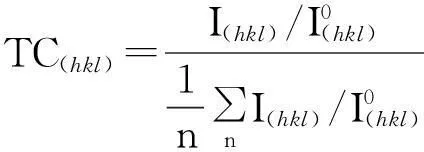
(1)

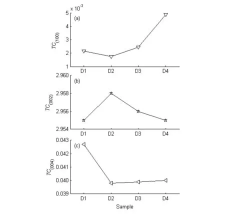
图3 GaZnO薄膜的织构系数Fig. 3 The values of TC(hkl) of the GaZnO thin films
图4(a)给出了不同薄膜厚度时GaZnO样品(002)衍射峰的半高宽(Δθ)数据,厚度对薄膜半高宽Δθ具有较为明显的影响,薄膜厚度增加时,Δθ逐渐减小,但当厚度大于510 nm时,Δθ则随之增大.可见,GaZnO样品的半高宽Δθ随厚度增大而呈现出先减后增的变化趋势.由于样品(002)衍射峰位的变化很小,因此半高宽Δθ的大小反映了薄膜结晶质量的好坏.基于XRD测试数据,GaZnO样品的晶粒尺寸t可以利用谢乐公式[44,45]进行计算:
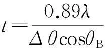
(2)
(2)式中,λ为X射线波长(λ=0.15406 nm),θB为最大衍射峰(002)晶面的Bragg角,Δθ为(002)衍射峰的半高宽.图4(b)为GaZnO样品的晶粒尺寸t随薄膜厚度变化的关系曲线,由图可见,薄膜厚度明显影响GaZnO样品的晶粒尺寸t,当厚度从320 nm增大到510 nm时,GaZnO样品的晶粒尺寸t迅速增大(97.8 nm),但当厚度进一步增大时,其晶粒尺寸t则明显减小.GaZnO薄膜开始生长时,由于薄膜与基片之间存在晶格不匹配,所以开始生长的薄膜存在较多的位错等晶体缺陷,导致GaZnO薄膜的结晶质量较差.随着薄膜厚度的增加,由于先生长的薄膜可以作为后生长薄膜的缓冲层,因此后生长的薄膜的位错等晶体缺陷大大减少,所以GaZnO薄膜的晶化程度显著提高,晶粒尺寸明显增大.上述结果表明:薄膜厚度对GaZnO样品的晶体质量具有明显的影响.
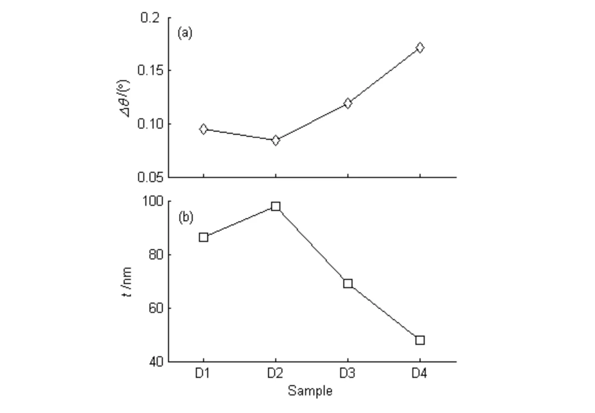
图4 GaZnO薄膜的半高宽和晶粒尺寸Fig. 4 The values of Δθ and t for the GaZnO thin films
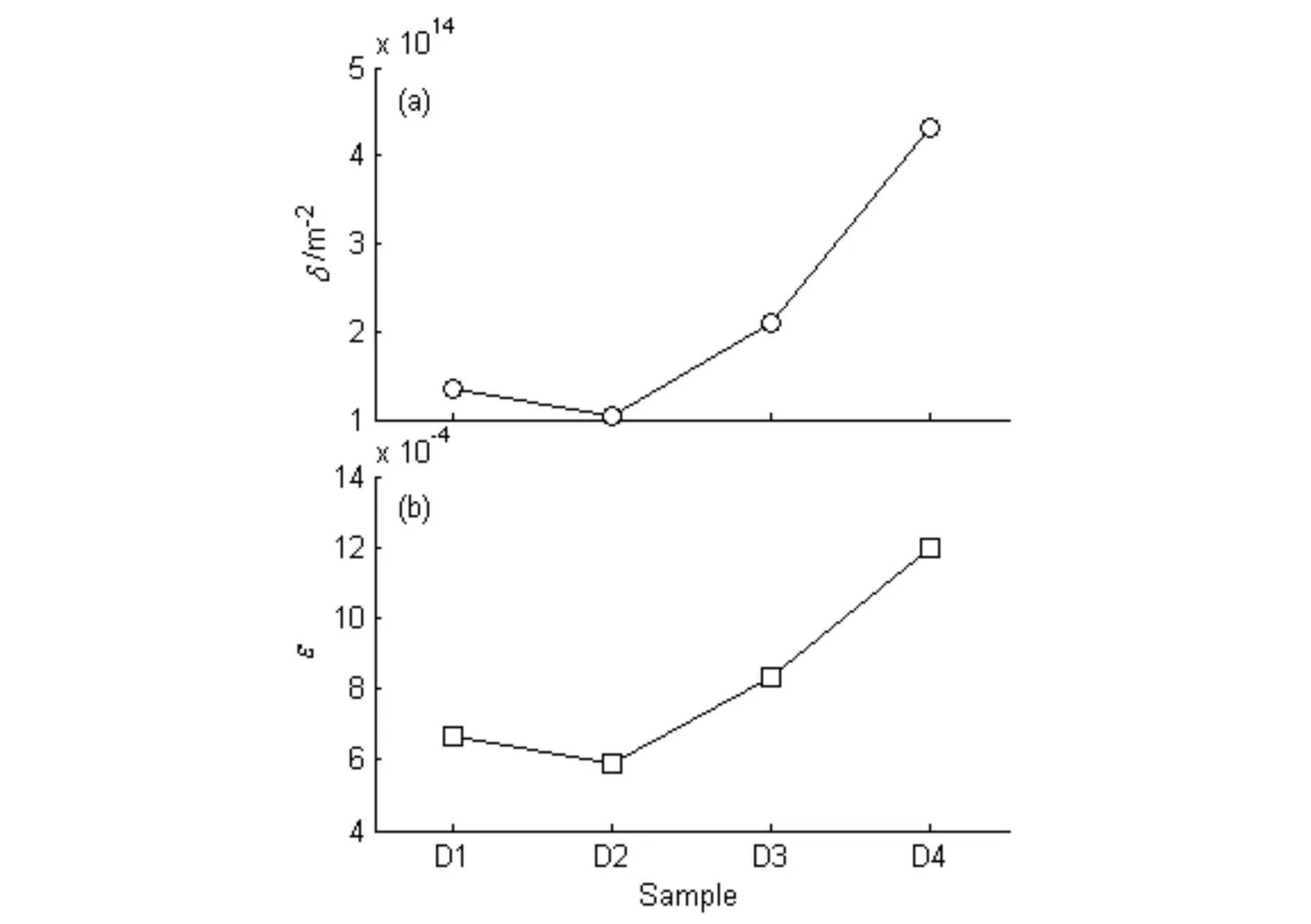
图5 GaZnO薄膜的位错密度和晶格应变Fig. 5 The values of δ and ε for the GaZnO thin films
GaZnO薄膜样品的位错密度(δ)和晶格应变(ε)可以根据下列公式[46,47]进行计算:

(3)

(4)
不同厚度时GaZnO薄膜样品的δ和ε数值如图5所示,可以看到,随着薄膜厚度的增加,δ和ε先减小后增大,它们呈现出相同的变化趋势,当薄膜厚度为510nm时,GaZnO样品D2具有最小的位错密度δ和晶格应变ε,分别为1.044×10¹⁴m-2和5.887×10⁻⁴.
GaZnO薄膜为六角纤锌矿结构,其晶格常数可以根据(5)式确定[48]:

(5)
(5)式中,a和c为晶格常数.对于(002)晶面,由(5)式可得:
(6)
对于(100)晶面,(5)式可变为:

(7)
另外,GaZnO薄膜样品的Zn-O键长(L)由公式(8)计算[49]:

(8)
(8)式中,a和c为样品的晶格常数,u与a、c之间的关系为[49]:
(9)
图6为不同薄膜厚度时GaZnO样品的晶格常数a、c和Zn-O键长L的数值,从图6看出,薄膜厚度增大时,参数a、c和L表现出相同的变化趋势,在实验研究的薄膜厚度范围内,a、c和L的数值范围分别为0.33424~0.33543 nm、0.52351~0.52475 nm和0.20201~0.20266 nm,相应的c/a比范围为1.56443~1.56629,这些结果与标准ZnO试样(JCPDS No. 36-1451)数据(a=0.32498、c=0.52066、L=0.19778、c/a=1.60213)基本一致.Srinivasan小组[50]和Anandan等人[51]在研究锂掺杂ZnO和钇掺杂ZnO薄膜时也有类似的报道.

图6 GaZnO薄膜的晶格常数和Zn-O键长Fig. 6 The values of a, c and L for the GaZnO thin films
3结语
采用Ga2O3:ZnO高密度陶瓷靶作为溅射材料,利用射频磁控溅射技术在玻璃基片上制备了GaZnO半导体薄膜,研究了薄膜厚度对GaZnO样品生长特性和微结构性能的影响.研究结果表明:所制备的GaZnO样品均为六角纤锌矿型的多晶结构,并表现出(002)晶面的择优取向生长特性.薄膜厚度对GaZnO样品的(002)取向性、晶化程度和微结构参数等具有明显的影响,随着薄膜厚度的增加,GaZnO样品的(002)择优取向程度和晶粒尺寸表现为先增大后减小的变化趋势,而半高宽、位错密度和晶格应变则呈现出先减小后增大的变化趋势.当薄膜厚度为510 nm时,GaZnO样品的晶粒尺寸最大为97.8 nm、织构系数TC(002)最高为2.959、半高宽最窄为0.084°、晶格应变最小为5.887×10⁻⁴、位错密度最低为1.044×10¹⁴m-2,同时所制备GaZnO样品的晶格常数和Zn-O键长均与标准样品相吻合.
参考文献
[1]Kim J Y, Lee K, Coates N E, et al. Tandem polymer solar cells fabricated by all-solution processing [J]. Science, 2007, 317 (5835): 222-225.
[2]Tang C W. Two-layer organic photovoltaic cell [J]. Appl Phys Lett, 1986, 48 (2): 183-185.
[3]李襄宏, 唐定国. 基于1,10-邻菲罗啉衍生物的两亲性钌配合物的合成及其光电转化性质 [J]. 中南民族大学学报(自然科学版), 2009, 28 (3): 9-13.
[4]顾锦华,龙路,兰椿,等.铝掺杂氧化锌薄膜的光学性能及其微结构研究[J].中南民族大学学报(自然科学版),2014,33(4):78-84.
[5]Sio A D, Chakanga K, Sergeev O, et al. ITO-free inverted polymer solar cells with ZnO:Al cathodes and stable top anodes[J]. Sol Energy Mater Sol Cells, 2012, 98 (1): 52-56.
[6]钟志有,兰椿,龙路,等.磁控溅射法制备ZnO:Ga薄膜的结晶质量及其应力研究[J].中南民族大学学报(自然科学版), 2015, 34 (1): 66-72.
[7]Burroughes J H, Bradley D D C, Brown A R, et al. Light-emitting diodes based on conjugated polymers [J]. Nature, 1990, 347 (6293): 539-541.
[8]Tang C W, VanSlyke S A. Organic electroluminescent diodes [J]. Appl Phys Lett, 1987, 51 (12): 913-915.
[9]Zhong Z Y, Jiang Y D. Surface treatments of indium-tin oxide substrates for polymer electroluminescent devices [J]. Phys Status Solidi A, 2006, 203 (15): 3882-3892.
[10]陈首部, 韦世良, 何翔, 等. 改性方法对氧化铟锡衬底表面形貌和化学组分的影响 [J]. 中南民族大学学报(自然科学版), 2009, 28 (4): 43-46.
[11]You Z Z, Hua G J, Lou S F. Optoelectrical characteristics of organic light-emitting devices fabricated with different cathodes [J]. Int J Electron, 2011, 98 (1): 129-135.
[12]顾锦华, 钟志有, 何翔, 等. 真空退火处理对光敏薄膜及聚合物太阳电池性能的影响[J]. 中南民族大学学报(自然科学版), 2009, 28 (3): 30-33.
[13]Kim H, Horwitz J S, Kim W H, et al. Doped ZnO thin films as anode materials for organic light-emitting diodes[J]. Thin Solid Films, 2002, 420-421 (1): 539-543.
[14]Cao H T, Sun C, Pei Z L, et al. Properties of transparent conducting ZnO:Al oxide thin films and their application for molecular organic light-emitting diodes[J]. J Mater Sci: Mater Electron, 2004, 14 (1): 169-174.
[15]Kim H, Piqué A, Horwitz J S, et al. Effect of aluminum doping on zinc oxide thin films grown by pulsed laser deposition for organic light-emitting devices[J]. Thin Solid Films, 2000, 377-378: 798-802.
[16]孙奉娄, 惠述伟. 衬底温度对射频溅射沉积ZAO透明导电薄膜性能的影响 [J]. 中南民族大学学报(自然科学版), 2009, 28 (2): 10-13.
[17]Kim J J, Lee J H, Ba J Y, et al. Characteristics of low-temperature-annealed ZnO-TFTs [J]. J Korean Phys Soc, 2010, 56 (1): 404-408.
[18]Shim J H, Choi J H, Lee C M, et al. Fabrication and comparison of the properties of SnInZnO and InZnO TFTs processed by using the sol-gel method [J]. J Korean Phys Soc, 2010, 57 (6): 1847-1851.
[19]Patel N G, Patel P D, Vaishnav V S. Indium tin oxide (ITO) thin film gas sensor for detection of methanol at room temperature [J]. Sensor Actuat B-Chem, 2003, 96 (1-2): 180-189.
[20]Yi I-J, Kim J-H, Choi Y J, et al. A disposable biosensor with Prussian blue deposited electrode [J]. Microelectron Eng, 2006, 83 (4-9): 1594-1597.
[21]Mitsubayashi K, Wakabayashi Y, Tanimoto S, et al. Optical-transparent and flexible glucose sensor with ITO electrode [J]. Biosens Bioelectron, 2003, 19 (1): 67-71.
[22]Minami T. Present status of transparent conducting oxide thin-film development for indium-tin-oxide (ITO) substitutes [J]. Thin Solid Films, 2008, 516 (17): 5822-5828.
[23]Guo J, Zheng J, Song X, et al. Synthesis and conductive properties of Ga-doped ZnO nanosheets by the hydrothermal method [J]. Mater Lett, 2013, 97 (1): 34-36.
[24]Rao T P, Kumar M C S, Hussain N S. Effects of thickness and atmospheric annealing on structural, electrical and optical properties of GZO thin films by spray pyrolysis [J]. J Alloy Compd, 2012, 541 (1): 495-504.
[25]Reddy K T R, Reddy T B S, Forbes I, Miles R W. Highly oriented and conducting ZnO:Ga layers grown by chemical spray pyrolysis [J]. Surf Coat Technol, 2002, 151-152 (1): 110-113.
[26]Minami T, Miyata T, Ohtani Y, et al. Effect of thickness on the stability of transparent conducting impurity-doped ZnO thin films in a high humidity environment [J]. Phys Status Solidi R, 2007, 1(1): R31-R33.
[27]Kim H, Horwitz J S, Kim W H, et al. Doped ZnO thin films as anode materials for organic light-emitting diodes[J]. Thin Solid Films, 2002, 420-421 (1): 539-543.
[28]Wang L, Swensen J S, Polikarpov E, et al. Highly efficient blue organic light-emitting devices with indium-free transparent anode on flexible substrates [J]. Org Electron, 2010, 11 (9): 1555-1560.
[29]Gorrie C W, Sigdel A K, Berry J J, et al. Effect of deposition distance and temperature on electrical, optical and structural properties of radio-frequency magnetron-sputtered gallium-doped zinc oxide [J]. Thin Solid Films, 2010, 519 (1): 190-196.
[30]Liu H, Fang L, Tian D, et al. Different magnetothermo-
electric behavior in Al- and Ga-doped ZnO thin films [J]. J Alloy Compd, 2014, 588 (1): 370-373.
[31]Kim Y H, Jeong J, Lee K S, et al. Effect of composition and deposition temperature on the characteristics of Ga doped ZnO thin films [J]. Appl Surf Sci, 2010, 257 (1): 109-115.
[32]Bie X, Lu J, Wang Y, et al. Optimization of parameters for deposition of Ga-doped ZnO films by DC reactive magnetron sputtering using Taguchi method [J]. Appl Surf Sci, 2011, 257 (14): 6125-6128.
[33]Park H-K, Kang J-W, Na S-I, et al. Characteristics of indium-free GZO/Ag/GZO and AZO/Ag/AZO multilayer electrode grown by dual target DC sputtering at room temperature for low-cost organic photovoltaics [J]. Sol Energy Mater Sol Cells, 2009, 93 (11): 1994-2002.
[34]Lin Y C, Yen W T, Shen C H, et al. Surface texturing of Ga-doped ZnO thin films by pulsed direct-current magnetron sputtering for photovoltaic applications [J]. J Electron Mater, 2012, 41(3): 442-450.
[35]Tsay C-Y, Wu C-W, Lei C-M, et al. Microstructural and optical properties of Ga-doped ZnO semiconductor thin films prepared by sol-gel process [J]. Thin Solid Films, 2010, 519 (5): 1516-1520.
[36]Tsay C-Y, Fan K-S, Lei C-M. Synthesis and characteri-
zation of sol-gel derived gallium-doped zinc oxide thin films [J]. J Alloy Compd, 2012, 512 (1): 216-222.
[37]Nam T, Lee C W, Kim H J, et al. Growth characteristics and properties of Ga-doped ZnO (GZO) thin films grown by thermal and plasma-enhanced atomic layer deposition [J]. Appl Surf Sci, 2014, 295 (1): 260-265.
[38]Saito K, Hiratsuka Y, Omata A, et al. Atomic layer deposition and characterization of Ga-doped ZnO thin films [J]. Superlattice Microst, 2007, 42 (1-6): 172-175.
[39]You Z Z, Hua G J. Structural, optical and electrical characterization of ZnO:Ga thin films for organic photovoltaic applications[J]. Mater Lett, 2011, 65 (21-22): 3234-3236.
[40]陈首部.掺锡氧化铟导电玻璃的表面改性及其性能研究[J].中南民族大学学报(自然科学版), 2014, 33 (2): 57-62.
[41]Raoufi D, Raoufi T. The effect of heat treatment on the physical properties of sol-gel derived ZnO thin films [J]. Appl Surf Sci, 2009, 255 (11): 5812-5817.
[42]Zhong Z Y, Zhang T. Microstructure and optoelectronic properties of titanium-doped ZnO thin films prepared by magnetron sputtering [J]. Mater Lett, 2013, 96 (1): 237-239.
[43]Valle G G, Hammer P, Pulcinelli S H, et al. Transparent and conductive ZnO:Al thin films prepared by sol-gel dip-coating [J]. J Eur Ceram Soc, 2004, 24 (4): 1009-1013.
[44]Hong R, Shao J, He H, et al. ZnO:Zn phosphor thin films prepared by face-to-face annealing [J]. J Cryst Growth, 2005, 284 (3-4): 347-352.
[45]黄涛, 李灿, 吴静, 等. 四方形钯纳米片的控制合成 [J]. 中南民族大学学报(自然科学版), 2013, 32 (3): 5-7.
[46]Matheswaran P, Gokul B, Abhirami KM, et al. Thickness dependent structural and optical properties of In/Te bilayer thin films [J]. Mater Sci Semicond Process, 2012, 15 (5): 486-491.
[47]Arivazhagan V, Parvathi M M, Rajesh S. Impact of thickness on vacuum deposited PbSe thin films [J], Vacuum, 2012, 86 (8): 1092-1096.
[48]Zhang T, Zhong Z. Effect of working pressure on the structural, optical and electrical properties of titanium-gallium co-doped zinc oxide thin films[J]. Mater Sci-Poland, 2013, 31 (3): 454-461.
[49]Murtaza G, Ahmad R, Rashid M S, et al. Structural and magnetic studies on Zr doped ZnO diluted magnetic semiconductor [J]. Curr Appl Phys, 2014, 14 (2): 176-181.
[50]Srinivasan G, Kumar R T R, Kumar J. Li doped and undoped ZnO nanocrystalline thin films: a comparative study of structural and optical properties [J]. J Sol-Gel Sci Technol, 2007, 43 (2): 171-177.
[51]Anandan S, Muthukumaran S. Influence of Yttrium on optical, structural and photoluminescence properties of ZnO nanopowders by sol-gel method [J]. Opt Mater, 2013, 35 (12): 2241-2249.
中图分类号TM914
文献标识码A
文章编号1672-4321(2016)01-0075-06
基金项目湖北省自然科学基金资助项目(2011CDB418); 中央高校基本科研业务费专项资金资助项目(CZW14019)
作者简介钟志有(1965-), 男, 教授, 博士, 研究方向: 光电信息功能材料与器件, E-mail: zhongzhiyou@163.com
收稿日期2015-11-18
猜你喜欢
工程塑料应用(2022年11期)2022-11-23
农业工程学报(2022年10期)2022-08-22
陶瓷学报(2021年2期)2021-07-21
湖北农机化(2020年4期)2020-07-24
科学导报(2020年86期)2020-01-13
表面工程与再制造(2019年3期)2019-12-04
制造技术与机床(2019年6期)2019-06-25
表面技术(2019年2期)2019-02-26
表面技术(2019年2期)2019-02-26
制造技术与机床(2017年3期)2017-06-23
