
First-principles investigations on the mechanical,thermal, electronic,and optical properties of the defect perovskites Cs2Sn X6(X=Cl,Br,I)∗
2017-08-30 08:26HaiMingHuang黄海铭ZhenYiJiang姜振益andShiJunLuo罗时军
Chinese Physics B 2017年9期
关键词:黄海
Hai-Ming Huang(黄海铭),Zhen-Yi Jiang(姜振益),and Shi-Jun Luo(罗时军)
1 Shaanxi Key Laboratory for Theoretical Physics Frontiers,Institute of Model Physics, Northwest University,Xi’an 710069,China
2 School of Science,Hubei University of Automotive Technology,Shiyan 442002,China
First-principles investigations on the mechanical,thermal, electronic,and optical properties of the defect perovskites Cs2Sn X6(X=Cl,Br,I)∗
Hai-Ming Huang(黄海铭)1,2,Zhen-Yi Jiang(姜振益)1,†,and Shi-Jun Luo(罗时军)2
1 Shaanxi Key Laboratory for Theoretical Physics Frontiers,Institute of Model Physics, Northwest University,Xi’an 710069,China
2 School of Science,Hubei University of Automotive Technology,Shiyan 442002,China
The mechanical properties,thermal properties,electronic structures,and optical properties of the defect perovskites Cs2Sn X6(X=Cl,Br,I)were investigated by first-principles calculation using PBE and HSE06 hybrid functional.The optic band gaps based on HSE06 are 3.83 eV for Cs2SnCl6,2.36 eV for Cs2SnBr6,and 0.92 eV for Cs2SnI6,which agree with the experimental results.The Cs2SnCl6,Cs2SnBr6,and Cs2SnI6are mechanically stable and they are all anisotropic and ductile in nature.Electronic structures calculations show that the conduction band consists mainly of hybridization between the halogen p orbitals and Sn 5s orbitals,whereas the valence band is composed of the halogen p orbitals.Optic properties indicate that these three compounds exhibit good optical absorption in the ultraviolet region,and the absorption spectra red shift with the increase in the number of halogen atoms.The defect perovskites are good candidates for probing the lead-free and high power conversion efficiency of solar cells.
first-principles calculation,perovskites,elastic properties,optical properties
1.Introduction
Perovskites compounds,especially pure inorganic and inorganic/organic halides,such as CsSnI3,methyl ammonium lead iodide CH3NH3PbI3,and for mamidinium lead iodide HC(NH2)2PbI3,have been proved to be some of the most promising materials in solar cells.[1–3]The ABX3type halidebased hybrid per-ovskites,where A is a metal atom or molecular cation,B is Sn or Pb,and X is a halide atom(Cl,Br, or I),are attracting an increasing amount of attention for applications due to advantageous optical properties and high power conversion efficiency.[4–10]Since Miyasaka et al.[11]pioneered the incorporation of the hybrid organic–inorganic per-ovskite halides CH3NH3PbI3into solar cells,the power conversion efficiency of this kind of solar cell increased from the begging of 3.8%to the current 20.1%in a few years.[12]However,the presence of toxic elements and instabilities of these per-ovskites halides greatly limit their widespread applications in efficient field-effect transistors light-emitting diodes,and photovoltaic devices.[13–17]Therefore,looking for non-toxic, environmentally friendly,and high conversion efficiency of new per-ovskite-type solar cell materials has become a current research hotspot.
Recently,Falaras et al.[18]reported three defect perovskites compounds Cs2Sn X6(X=Cl,Br,I).They found Cs2SnCl6,Cs2SnBr6,and Cs2SnI6are all direct band gap semiconductors and can be used in dye-sensitized solar cells. They also found these three compounds are air-stable,and the dye-sensitized solar cells based on Cs2SnI6hole-transporting materials present a power conversion efficiency of 4.23%at 1 sun illumination.Neilson et al.[19]pointed out that the greatest advantage of this kind of defect perovskites is that the Cs2Sn X6compounds contain Sn4+rather than Sn2+in the B-site,which makes it more stable under exposure to air and moisture.However,Xiao[20]and colleagues indicated the real valence state of Sn in Cs2SnI6is+2 rather than+4.Although there are different opinions about the valence state of Sn cations in the defect perovskites compounds,it does not prevent the researchers from doing theoretical and experimental investigations on the new lead-free perovskite solar cell materials.[21–23]
The mechanical and thermal properties of perovskite are important for practical applications in solar cells.On the one hand,the absorption performances of perovskite solar cell strongly rely on the crystallinity and stress state of the perovskite layer.[24]On the other hand,as very important thermal parameters,the Debye temperature and melting temperature are related to the bond strength,which is important for the preparation of solar cell devices.Therefore,it is essential to study the mechanical and thermal properties of perovskite type solar cell materials.In this paper,we study the structural, mechanical,thermal,electronic and optical properties of the defect perovskites Cs2Sn X6(X=Cl,Br,I)by first-principlescalculations.Our findings shed light on the key properties that are hard to measure experimentally and probing the lead-free solar cells materials.
2.Computational details
First-principles calculations were carried out to study various physical properties of the defect perovskites by using the Vienna ab initio simulation package(VASP).[25]Generalized gradient approximation(GGA)of Perdew–Burke–Ernzerh(PBE)was used to describe the exchange-correlation functional.[26]It is well known that PBE usually underestimates the band-gap,which will result in unreasonable optic properties.In order to overcome this predicament,band gap correction was considered by using range separated hybrid functional(HSE06),[27]which can give improved approximate results to match with experimental data.The electronic configurations:6s1for Cs,5s25p2for Sn,3s23p5for Cl,4s24p5for Br,and 5s25p5for I were used in calculations.The plane wave cut-off energy was set to 450 eV.A mesh of 9×9×9 k-points was used for calculating the electronic,mechanical,thermal, and optic properties.The convergence tolerances of the energy and the force are 1.0×10⁻⁶eV and 1.0×10⁻²eV/˚A, respectively.
3.Results and discussion
3.1.Structural properties
Cs2Sn X6chemical composition presents the cubic anti-fluorite phase with the space group F m-3m in cubic structure as shown in Fig.1.In this structure,the defect perovskites Cs2Sn X6own the same structure with K2PtCl6,in which the isolated[Sn X6]2−anions octahedra bridged by Cs+cations, the Sn4+cations formed a face centered cubic lattice and are surrounded by an X6octahedral.[17,18,28]Firstly,a volume optimization process was carried out to predict the optimal structure.Calculated equilibrium lattice constants are summarized and compared with available theoretical and experimental data in Table 1.
One can observe that the optimized lattice constants of Cs2SnCl6are almost the same as those of the experimental results.However,there is a slight deviation for Cs2SnBr6and for Cs2SnI6,respectively.This slight deviation does not affect further research.On the whole,there is a good agreement between the optimized lattice constants and the experimental findings and available theoretical data.Furthermore, one can see that the lattice constants increase in the order from Cs2SnCl6to Cs2SnBr6to Cs2SnI6.The phenomenon is due mainly to the size differences between the univalent anion Cl−, Br−,and I−.
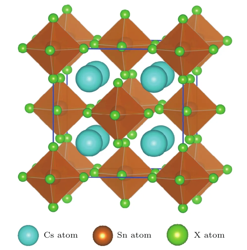
Fig.1.(color online)Crystal structure of the defect perovskites Cs2Sn X6(X=Cl,Br,I).Thick blue lines represent the unit cell edges.
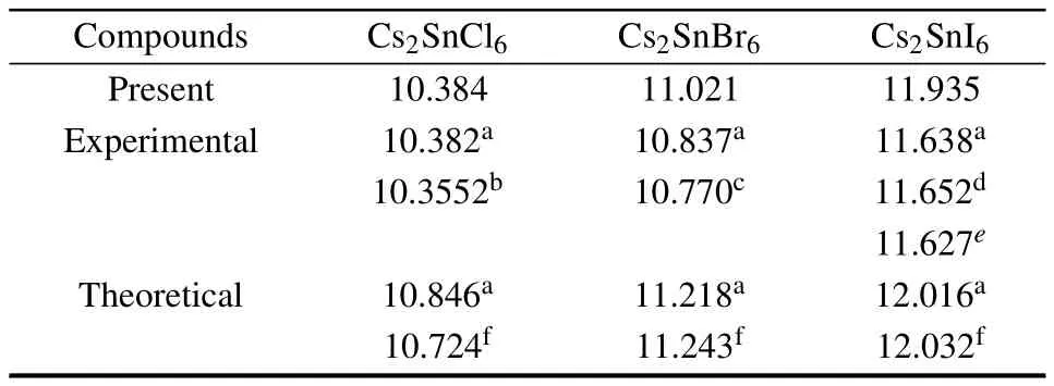
Table 1.Optimized lattice constants(˚A)of Cs2Sn X6(X=Cl,Br,I). Experimental and other theoretical values are included.
3.2.Mechanical properties
It is known that first-principles methods are often used to calculate reliable elastic properties of solid materials.The criterions for mechanical stability of cubic crystals are given by[33]
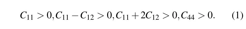
Table 2 summarizes the calculated elastic constants Cijof the defect perovskites Cs2Sn X6.One can see that the elastic constants satisfy these generalized stability criterions,indicating these three compounds are mechanically stable.Meanwhile,the elastic constant C11decreases from chlorine to bromine to iodine in Cs2Sn X6(X=Cl,Br,I),meaning that the trend of resistance one-way compression declines.Cs2SnCl6presents more strong resistance for one-way compression as compared to Cs2SnBr6and Cs2SnI6.At the same time,the value of elastic constant C44is less than that of C11,which indicates that their resistance to pure shear deformation is weaker than that of the one-way compression.
Using the elastic constants,some mechanical properties including shear anisotropy factor(A),bulk modulus(B),shear modulus(G),Pough’s ratio(B/G),Frantesvich ratio(G/B), Young’s modulus(Y),Poisson’s ratio(υ)and Kleinman parameter(ξ)are also calculated and presented in Table 2.The shear anisotropy factor A is used to decide the anisotropic or isotropic characteristic of a solid.In general,the shear anisotropic factor for isotropic crystals is A=1,while for anisotropic crystals it is A/=1.The shear anisotropic factors reported in Table 2 indicate Cs2Sn X6compounds are all anisotropic.It is clear that the level of anisotropy for Cs2SnBr6is the highest among these three defect perovskites. Pough’s ratio B/G and Frantesvich G/B ratio provide the brittleness or ductility of a compound.If B/G<1.75(G/B>0.571),the material is brittle,otherwise,the ductile behavior is predicted.[34]Present values of Pough’s ratio for Cs2SnCl6, Cs2SnBr6and Cs2SnI6are bigger than 1.75,therefore these defect perovskites are ductile in nature.
Young’s modulus Y is an important parameter in showing the stiffness of a solid material.The larger the Young’s modulus,the stiffer the solid material will be.From Table 2,it is clear that the Young’s modulus decreases with large anion size, indicting Cs2SnCl6is stiffer than Cs2SnBr6and Cs2SnI6,and the capability of resisting elastic deformation decreases from Cs2SnCl6to Cs2SnBr6to Cs2SnI6.Poisson’s ratio υ gives some informations about the character of force acting on solid materials.The forces among the atoms constituting the material are central if the value of υ lies between 0.25 and 0.50. The obtained Poisson ratio υ for Cs2SnCl6,Cs2SnBr6and Cs2SnI6are just in this range which means that interatomic forces in Cs2Sn X6are central.
3.3.Thermal properties
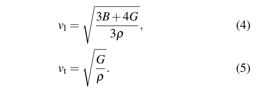
Debye temperature ΘDis a fundamental parameter for materials’thermodynamic properties,and it is closely related to specific heat,bond strength,elastic constants,and melting temperature.[35]ΘDcan be predicted by the average sound velocity Vmaccording to[33,36]
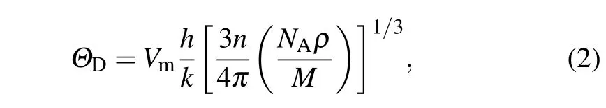
where h represents Plank’s constant,k is the Boltzman constant,n is the number of atoms per molecule,NAis the Avogadro number,ρ is the density of the solid,and M represents the molecular weight.The average sound velocity Vmwas calculated by[33,36]

where vtand vlare the transverse and longitudinal sound velocity,respectively,which is calculated by[37]
The calculated Debye temperatures of Cs2Sn X6(X=Cl, Br,I)are also listed in Table 2.Obviously,the values of Debye temperature ΘDdecrease in the following sequence: Cs2SnCl6>Cs2SnBr6>Cs2SnI6.The Cs2SnCl6presents the highest Debye temperature indicating the higher melting temperature.At present,there are no theoretical calculations as well as experimental measurements reported on the Debye temperature for Cs2SnCl6and Cs2SnBr6.However,there is a large deviation for the Debye temperature of Cs2SnI6between the present work 96.8 K and experimental result 149 K obtained by heat capacity data.[18]The main reason is the difference of lattice constant between theoretical calculations and experimental measurement.In general,the lattice constant has an important influence on the calculation of Debye temperature.As a comparison,we use the experimental lattice constant of 11.6527˚A[22]to calculate the Debye temperature of Cs2SnI6;the obtained value of ΘD=141.2 K is very close to the experimental results.
The Deby temperature corresponds to the highest frequency of the lattice vibration,which is actually a reflection of the strongest bonding of the crystal.Recently,Kumar et al.[38]obtained a linear relation between Deby temperature and melting temperature for II–VI and III–V semiconductors. In general,for the same compound,a larger Debye temperature means a higher melting temperature.[39]The melting temperature Mtof Cs2Sn X6can be calculated by elastic constants C11according to the following expression:[33,40]
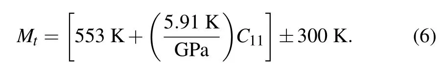
Calculated melting temperatures are also shown in Table 2.It is clear that the melting temperature of Cs2SnCl6is higher than that of Cs2SnCl6and Cs2SnBr6.The results are in agreement with the results of Debye temperature.
3.4.Electronic properties
Density of states and band structures calculations predict the direct band gaps at the Γ point for Cs2SnCl6,Cs2SnBr6and Cs2SnI6.The results are consistent with the ones of other investigators.[18,22]Band gap values,as obtained by PBE and HSE06 using the optimized lattice constants,are listed in Table 3.Obviously,the HSE06 results are a lot closer to the experimental measurements as compared to the PBE ones.The band structure of Cs2SnCl6indicates a band gap of 3.83 eV, which consists with the experimentally measured optical gap of 3.9 eV and is better than other theoretical calculations.For the Cs2SnBr6and Cs2SnI6,the direct band gaps are 2.36 and 0.92 eV,respectively,which is lower than the experimentally measured optical gap.There are two main reasons for this discrepancy:one is the difference of lattice constants between theoretical calculations and experimentally measured ones,the other arises from the fact that first-principles calculations often underestimate the band gap.
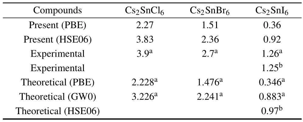
Table 3.Calculated band gap(eV)of Cs2 Sn X6(X=Cl,Br,I)using the PBE and HSE06 functional.Experimental and other theoretical values are also included.

Fig.2.(color online)(a)Band structures,(b)total and orbital-projected densities of states for Cs2SnCl6 based on the HSE06.
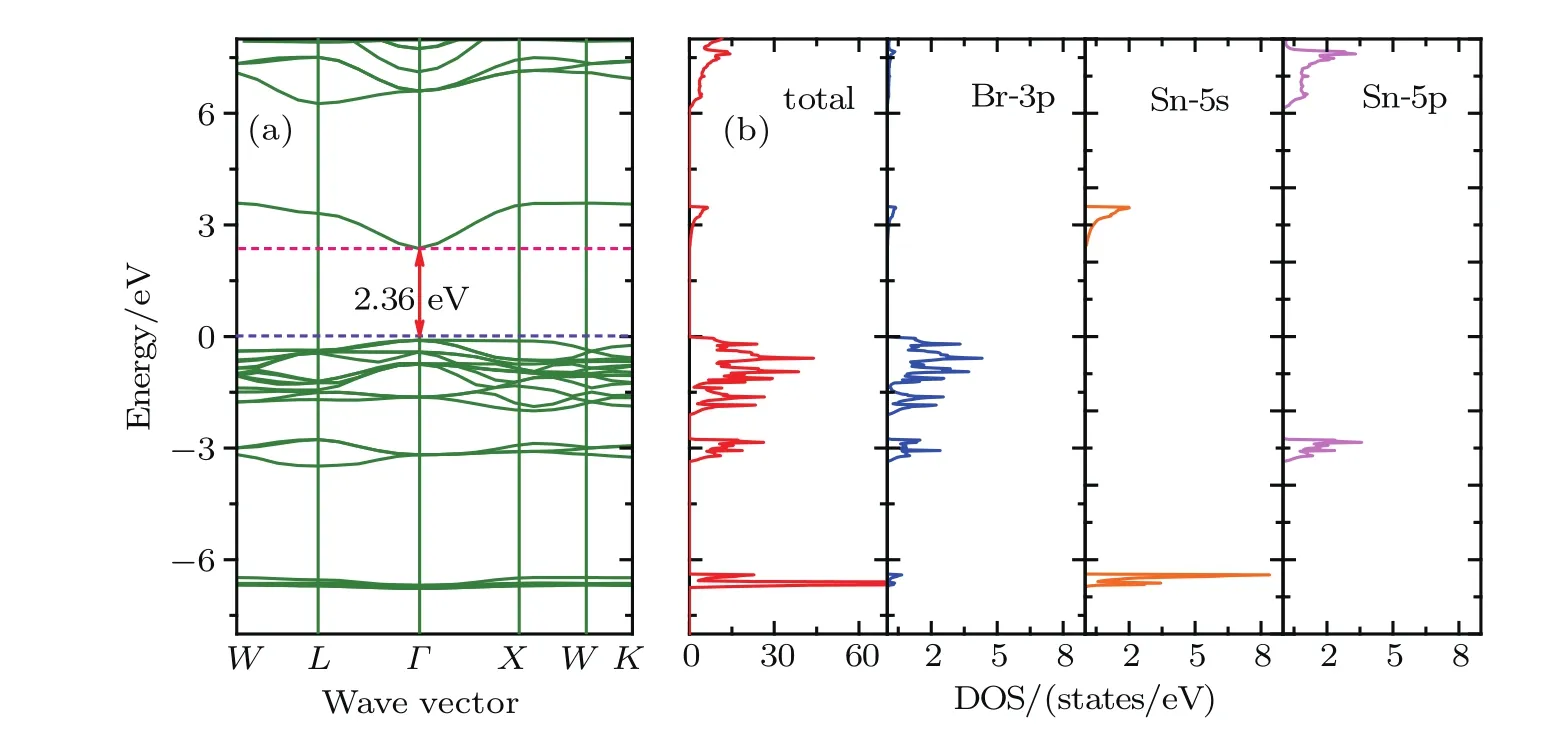
Fig.3.(color online)(a)Band structures,(b)total and orbital-projected densities of states for Cs2SnBr6 based on the HSE06.
Figures 2–4 present the band structures,total and orbital projected densities of states(DOSs)for title compounds based on the HSE06.We have not plotted the projected DOS of Cesium since its negligible contribution to the total DOS.It is clear that these three compounds have very similar electronic structures as well as a delicate difference.The orbital-projected DOSs indicate that the conduction band near the Fermi level is mainly composed of halogen p orbitals hybridized with Sn 5s orbitals,and the upper conduction bands, starting from 7.66,6.12 and 4.38 eV for Cs2SnCl6,Cs2SnBr6and Cs2SnI6,respectively.There is a forbidden gap of 2.86 eV for Cs2SnCl6,2.85 eV for Cs2SnBr6and 2.36 eV for Cs2SnI6between the two conduction bands.On the other hand,the valence band is constituted of the halogen p orbitals,and their band widths are 1.99 eV for Cs2SnCl6,2.08 eV for Cs2SnBr6and 2.22 eV for Cs2SnI6,respectively.Another halogen p orbital presents hybridization with Sn 5p orbital between−3.40 to−2.75 eV.In a deeper band,from−5.91 eV to−5.59 eV for Cs2SnCl6,from−6.73 eV to−6.39 eV for Cs2SnBr6and from−6.95 eV to−6.67 eV for Cs2SnI6,the valence band is mainly made of the Sn 5s orbital.
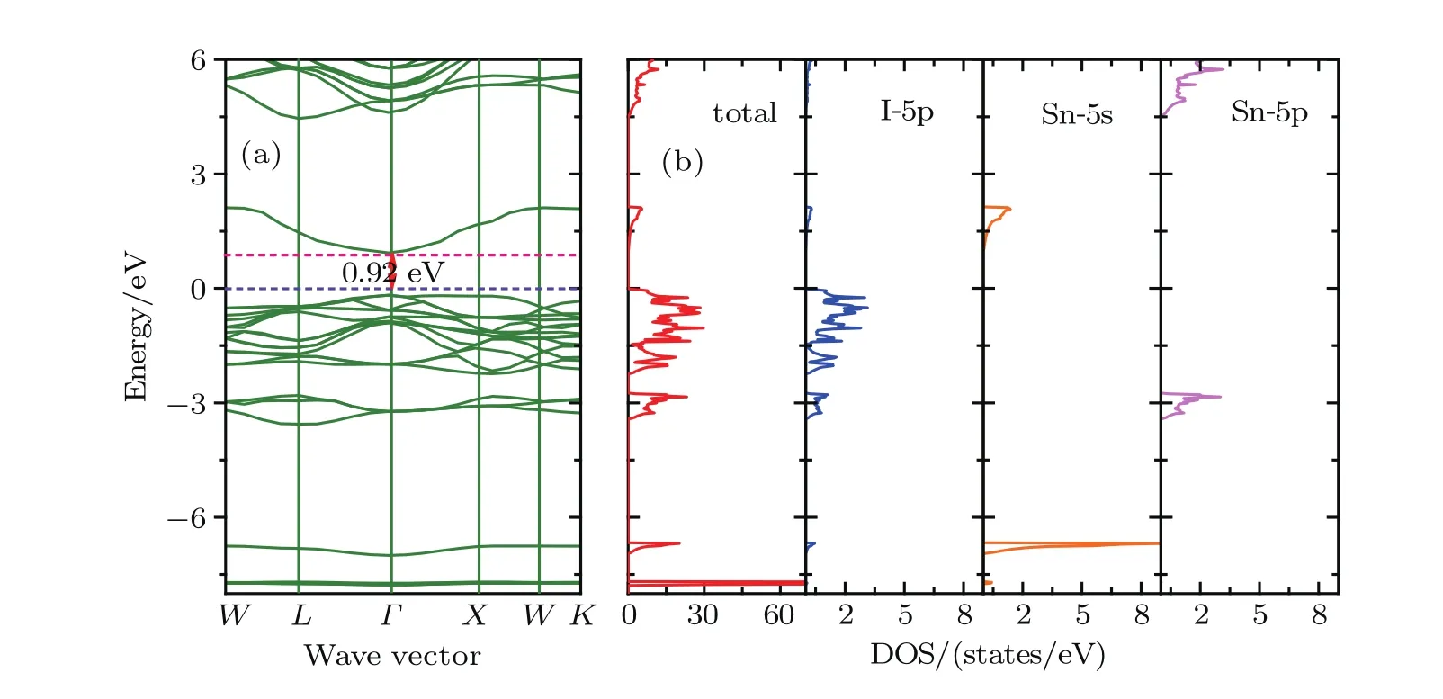
Fig.4.(color online)(a)Band structures,(b)total and orbital-projected densities of states for Cs2SnI6 based on the HSE06.
3.5.Optic properties
The optical properties of a semiconductor material are closely related to their electronic band structures;it is usually obtained from the dielectric function by the formula that is given by[41,42]
where ω is the angular frequency,and ε1(ω)and ε2(ω)are the real and the imaginary parts of the complex dielectric function, respectively.
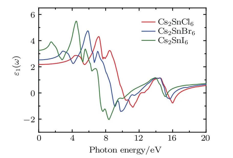
Fig.5.(color online)Real part of the dielectric function for the defect perovskites Cs2Sn X6(X=Cl,Br,I).
The dielectric functions of Cs2SnCl6,Cs2SnBr6,and Cs2SnI6with changes in photon energy were calculated up to 20.0 eV and shown in Figs.5 and 6.The static dielectric constants ε0(ω)are 2.17 for Cs2SnCl6,2.53 for Cs2SnBr6, and 3.26 for Cs2SnI6and the values increase with increasing halogen atomic number.The real part ε1(ω)is positive up to 10.1 eV,8.70 eV,and 7.23 eV for Cs2SnCl6,Cs2SnBr6, and Cs2SnI6,respectively.In this area,for Cs2SnI6,the real part has three peaks located at 4.39,7.15,and 8.45 eV.For Cs2SnBr6,it presents several peaks at 2.92,5.93,and 7.03 eV. Also for Cs2SnI6,its three peaks are located at 1.48,4.46,and 5.58 eV.
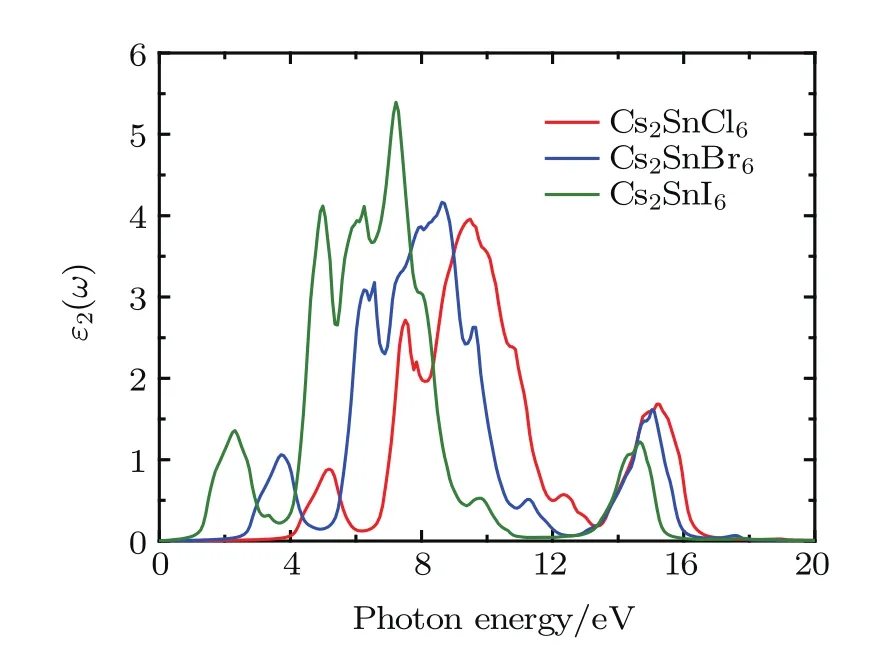
Fig.6.(color online)Imaginary part of the dielectric function for the defect perovskites Cs2 Sn X6(X=Cl,Br,I).
The imaginary dielectric function ε2(ω)gives some important information on the multifarious interband transitions between the valence and conduction bands.The imaginary part for Cs2SnCl6exhibits five major absorption peaks at 3.80, 5.19,7.50,9.49,and 15.23 eV.The five major absorption peaks of Cs2SnBr6are located at 2.32,3.74,6.54,8.65,and 15.05 eV.The five major absorption peaks of Cs2SnI6are located at 0.90,2.30,4.98,7.26,and 14.63 eV.These peaks are associated with the transition from valence bands to conduction ones.The lower energy peaks are relative to the electronic transition between the Cl-3p,Br-4p,and I-5p states in the upper valence bands and the Sn-5s states in conduction bands.
In addition to the real and imaginary components of the dielectric functions,the refractive index n(ω),extinction coefficient k(ω),absorption coefficient α(ω),reflectivity coefficient R(ω),optical conductivity κ(ω)and energy loss function L(ω)are calculated and plotted in Fig.7.Refractive index is an indispensable parameter to describe the optical properties of materials and has an important impact on optic devices such as solar cell and detectors.[43]From Fig.7(a),the curves of the refractivity index of Cs2SnCl6,Cs2SnBr6and Cs2SnI6coincide with the real part of the dielectric functions.The static refractive index n(0)for low frequency at 0 eV and their peak values are presented in Table 4.It is clear that the n(0)and peak values increase with the increasing of the size of halogen anions.Extinction coefficient k(ω)describes the attenuation of an electromagnetic wave in a material.In the low energy infrared region in Fig.7(b),the value of the extinction coefficient is close to zero,which indicates these three defect perovskites are transmitted to the infrared spectrum.
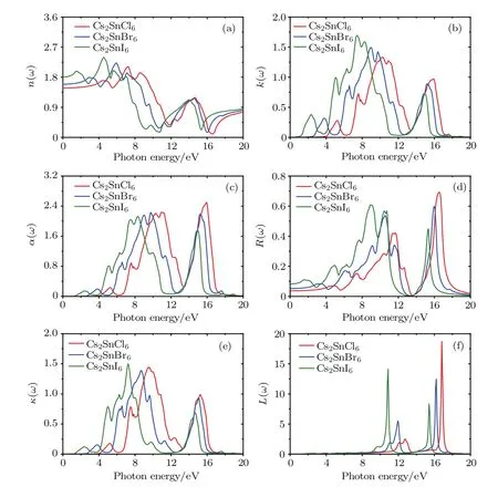
Fig.7.(color online)Refractive index n(ω),extinction coefficient k(ω),absorption coefficient α(ω),reflectivity coefficient R(ω), optical conductivity κ(ω)and energy loss function L(ω)of the defect perovskites Cs2Sn X6(X=Cl,Br,I).
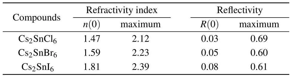
Table 4.Static refractive index,static reflectivity,maximum refractive index and maximum reflectivity for Cs2Sn X6(X=Cl,Br,I).
The absorption coefficient can be further calculated according to the refractive index and extinction coefficient.From Fig.7(c),one can see that the absorption edges are located at 3.96,2.52,and 1.07 eV for Cs2SnCl6,Cs2SnBr6,and Cs2SnI6, respectively.These absorption edge values are near the corresponding band gaps as predicted by the HSE06 method. The absorption spectrum of the intrinsic defect perovskites Cs2Sn X2is mainly concentrated in the ultraviolet region.With the increase of the number of halogen atoms,the absorption spectra have an obvious red shift,which means the Cs2SnI2is a promising material for photoelectric conversion.Moreover, there are five obvious characteristic peaks in the absorption spectrum.The positions of the peaks and the absorption edges are all presented in Table 5.Obviously,the position moves towards a low energy area with the increasing size of the halogen ions,and the strongest peak is located at15.9 eV for Cs2SnCl6, 9.73 eV for Cs2SnBr6,and 8.29 eV for Cs2SnI6,respectively. In the low energy range,the absorption coefficient is close to zero,indicating that its absorption of light waves in the low energy range is not obvious.
The static reflectivity R(0)and the maximum reflectivity of the title compounds are listed in Table 4.Figure 7(d) depicts the curves of reflectivity as a functional of photon energy.It is clear that the zero frequency reflectivity increases in the following sequence:Cs2SnCl6<Cs2SnBr6<Cs2SnI6.The reflectivity for these three compounds in the infrared region is lower than 8.0%reflecting the case that the effect of surface reflection and internal grain boundary reflection on the low energy infrared wave band is small.The wavelength of the maximum reflectivity is obtained around 74.95 nm for Cs2SnCl6, 77.69 nm for Cs2SnBr6,and 138.9 nm for Cs2SnI6,respectively.
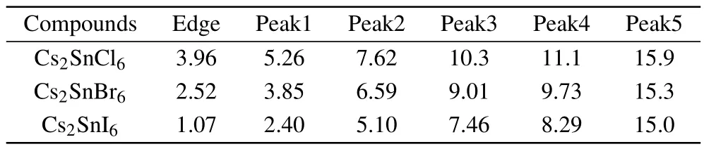
Table 5.The positions(eV)of the characteristic peaks and the absorption edges in the absorption spectrum for Cs2Sn X6(X=Cl,Br,I).
The optical conductivity,which is decided by refractive index and absorption coefficient,is usually used to investigate the optical response of material.From Fig.7(e),one can see that the optical conductivity follows the same trend as that of the absorption coefficient with increasing phonon energy.The optical conductivity of Cs2SnCl6is zero when the phonon energy is smaller than 3.96 eV and bigger than 17.59 eV.For Cs2SnBr6,the optical conductivity is zero when the phonon energy is smaller than 2.52 eV and bigger than 18.10 eV.Also for Cs2SnI6,the optical conductivity is zero when the phonon energy is smaller than 1.07 eV and bigger than 19.87 eV.The maximum optical conductivity appears when the energy is 9.51,8.71,and 7.24 eV for Cs2SnCl6,Cs2SnBr6,and Cs2SnI6, respectively.
The energy loss function is an important parameter in describing the energy loss when electrons pass through a dielectric.The function is directly relative to the real and imaginary components of dielectric functions,and the peak of the loss function is associated with plasma oscillation.Figure 7(f)depicts the energy loss function as a function of photon energy. One can see that the energy loss in two regions is very large, and the maximum energy loss points are located at 16.85, 16.23,and 10.85 eV for Cs2SnCl6,Cs2SnBr6,and Cs2SnI6u, respectively.The electronic energy loss for these three compounds is close to zero when the energy is bigger than 20.0 eV.
4.Conclusion
Employing the first-principles method within the PBE and HSE06 functional,we carried out a comprehensive study on the structural,mechanical,thermal,electronic,and optical properties of the defect per-ovskites Cs2SnCl6,Cs2SnBr6,and Cs2SnI6.The results indicate that the optimized lattice parameters are in good agreement with the available theoretical and experimental data.These three compounds are mechanically stable and they are all anisotropic and ductile in nature.Calculated Debye temperature and melting temperature decrease from Cs2SnCl6to Cs2SnBr6to Cs2SnI6.Density of states and band structures indicate direct band gaps for all the defect per-ovskites Cs2Sn X6,which accords with other theoretical investigations.Orbital-projected DOSs indicate that the contribution to the conduction band mainly originates from the halogen p orbitals hybridized with Sn 5s orbitals,whereas the contribution to the valence band is consisted of the halogen p orbitals. Some parameters,which are closely related to optical properties such as dielectric functions,refractive index,extinction coefficient,absorption coefficient,reflectivity coefficient,optical conductivity,and energy loss function,are studied theoretically for the first time.The results indicate that these three materials exhibit good optical absorption in the ultraviolet region,and the absorption spectra red shift with the increase of the number of halogen atoms.In conclusion,these three defect per-ovskites are good candidates for probing the lead-free and high-power conversion efficiency of solar cells materials owing to their stable mechanical properties and excellent optical absorption in the ultraviolet region.
[1]Chung I,Lee B,He J,Chang R P H and Kanatzidis M G 2012 Nature 485 486
[2]Baikie T,Fang Y,Kadro J M,Schreyer M,Wei F,Mhaisalkar S G, Graetzeld M and Whitec T J 2013 J.Mater.Chem.A 1 5628
[3]Zhou H,Chen Q,Li G,Luo S,Song T B,Duan H S,Hong Z,You J, Liu Y and Yang Y 2014 Science 345 542
[4]Brivio F,Walker A B and Walsh A 2013 APL Mater.1 042111
[5]Eperon G E,Patern`o G M,Sutton R J,Zampetti A,Haghighirad A A, Cacialli F and Snaith H J 2015 J.Mater.Chem.A 3 19688
[6]Weller M T,Weber O J,Henry P F,Di Pumpo A M and Hansen T C 2015 Chem.Commun.51 4180
[7]Lee C,Hong J,Stroppa A,Whangbo M H and Shim J H 2015 RSC Adv. 5 78701
[8]Feng J and Xiao B 2014 J.Phys.Chem.C 118 19655
[9]Yuan Y,Xu R,Xu H T,Hong F,Xu F and Wang L J 2015 Chin.Phys. B 24 116302
[10]Du H J,Wang W C and Zhu J Z 2016 Chin.Phys.B 25 108803
[11]Kojima A,Teshima K,Shirai Y and Miyasaka T 2009 J.Am.Chem. Soc.131 6050
[12]Boix P P,Agarwala S,Koh T M,Mathews N and Mhaisalkar S G 2015 J.Phys.Chem.Lett.6 898
[13]Lora da Silva E,Skelton J M,Parker S C and Walsh A 2015 Phys.Rev. B 91 144107
[14]Szafranski M and Katrusiak A 2016 J.Phys.Chem.Lett.7 3458
[15]Yi H T,Wu X X,Zhu X Y and Podzorov V 2016 Adv.Mater.28 6509
[16]Chen Z,Wang J J,Ren Y,Yu C and Shum K 2012 Appl.Phys.Lett.101 093901
[17]Qiu X F,Cao B Q,Yuan S,Chen X F,Qiu Z W,Jiang Y N,Ye Q,Wang H Q,Zeng H B,Liu J and Kanatzidis M G 2017 Sol.Energy Mater.Sol. Cells 159 227
[18]Kaltzoglou A,Antoniadou M,Kontos A G,Stoumpos C C,Perganti D, Siranidi E,Raptis V,Trohidou K N,Psycharis V,Kanatzidis M G and Falaras P 2016 J.Phys.Chem.C 120 11777
[19]Maughan A E,Ganose A M,Bordelon M M,Miller E M,Scanlon D O and Neilson J R 2016 J.Am.Chem.Soc.138 8453
[20]Xiao Z W,Lei H C,Zhang X,Zhou Y Y,Hosono H and Kamiya T 2015 Bull.Chem.Soc.Jpn.88 1250
[21]Lee B,Stoumpos C C,Zhou N J,Hao F,Malliakas C,Yeh C Y,Marks T J,Kanatzidis M G and Chang R P H 2014 J.Am.Chem.Soc.136 15379
[22]Xiao Z W,Zhou Y Y,Hosono H and Kamiya T 2015 Phys.Chem. Chem.Phys.17 18900
[23]Saparov B,Sun J P,Meng W W,Xiao Z W,Duan H S,Gunawan O, Shin D,Hill I G,Yan Y F and Mitzi D B 2016 Chem.Mater.28 2315
[24]Feng J 2014 APL Mater.2 081801
[25]Kresse G and Furthmuller J 1996 Comput.Mater.Sci.6 15
[26]Perdew J P,Burke K and Ernzerhof M 1996 Phys.Rev.Lett.77 3865
[27]Heyd J,Scuseria G E and Ernzerhof M 2006 J.Chem.Phys.124 219906
[28]Torres D T,Freire J D and Katiyar R S 1997 Phys.Rev.B 56 7763
[29]Brill T B,Gerhart R C and Welsh W A 1974 J.Magn.Reson.13 27
[30]Ketelaar J A A,Rietdijk A A and van Staveren C H 2010 Recl.Trav. Chim.Pays-Bas 56 907
[31]Stoumpos C C,Malliakas C D and Kanatzidis M G 2013 Inorg.Chem. 52 9019
[32]Wang G T,Wang D Y and Shi X B 2015 AIP Advances 5 127224
[33]Gu J B,Wang C J,Zhang W X,Sun Bin,Liu G Q,Liu D D and Yang X D 2016 Chin.Phys.B 25 126103
[34]Pugh S F 1954 Philos.Mag.45 823
[35]Duan Y H,Sun Y,Peng M J and Zhou S G 2014 J.Alloy.Compd.585 587
[36]Anderson O L 1963 J.Phys.Chem.Solids 24 909
[37]Mujica A and Needs R J 1996 J.Phys.:Conden.Matter 8 L237
[38]Kumar V,Jha V and Shrivastava A K 2010 Cryst.Res.Technol.45 920
[39]Lu W F,Li C J,Sarac B,S¸opu D,Yi J H,Tan J,Stoica M and Eckert J 2017 J.Alloy.Compd.705 445
[40]Fine M E,Brown M D and Marcus H L 1984 Scr.Metall.18 951
[41]Parvin R,Parvin F,Ali M S and Islam A K M A 2016 Chin.Phys.B 25 083101
[42]Fahad S,Murtaza G,Ouahrani T,Khenata R,Yousaf M,Omran S B and Mohammad S 2015 J.Alloy.Compd.646 211
[43]Zhao S,Lan C,Ma J,Pandey S S,Hayase S and Ma T 2015 Solid State Commun.213-214 19
29 March 2017;revised manuscript
22 May 2017;published online 31 July 2017)
10.1088/1674-1056/26/9/096301
∗Project supported by the National Natural Science Foundation of China(Grant Nos.51572219 and 11447030),the Natural Science Foundation of Shaanxi Province of China(Grant No.2015JM1018),and Graduate’s Innovation Fund of Northwest University of China(Grant No.YJG15007).
†Corresponding author.E-mail:jiangzy@nwu.edu.cn
©2017 Chinese Physical Society and IOP Publishing Ltd http://iopscience.iop.org/cpb http://cpb.iphy.ac.cn
猜你喜欢
大众健康(2022年4期)2022-04-27
幼儿画刊(2022年4期)2022-04-21
华人时刊(2020年21期)2021-01-14
作文小学中年级(2019年11期)2019-12-04
高中生之友(中旬刊)(2019年9期)2019-10-23
海峡姐妹(2019年8期)2019-09-03
湖北美术学院学报(2019年1期)2019-04-19
新高考·高三英语(2013年1期)2013-05-23
军事历史(1984年1期)1984-08-21

- Chinese Physics B的其它文章
- Improved control for distributed parameter systems with time-dependent spatial domains utilizing mobile sensor actuator networks∗
- Geometry and thermodynamics of smeared Reissner–Nordström black holes in d-dimensional AdS spacetime
- Stochastic responses of tumor immune system with periodic treatment∗
- Invariants-based shortcuts for fast generating Greenberger-Horne-Zeilinger state among three superconducting qubits∗
- Cancelable remote quantum fingerprint templates protection scheme∗
- A high-fidelity memory scheme for quantum data buses∗