
Spin-dependent transport characteristics of nanostructures based on armchair arsenene nanoribbons∗
2017-08-30 08:26KaiWeiYang杨开巍MingJunLi李明君XiaoJiaoZhang张小姣XinMeiLi李新梅YongLiGao高永立andMengQiuLong龙孟秋
Chinese Physics B 2017年9期
关键词:张小
Kai-Wei Yang(杨开巍),Ming-Jun Li(李明君),†,Xiao-Jiao Zhang(张小姣), Xin-Mei Li(李新梅),Yong-Li Gao(高永立),3,and Meng-Qiu Long(龙孟秋),‡
1 Hunan Key laboratory of Super Micro-structure and Ultrafast Process,School of Physics and Electronics,Central South University,Changsha 410083,China
2 Physical Science and Technology College of Yichun University,Yichun 336000,China
3 Department of Physics and Astronomy,University of Rochester,Rochester,NY 14627,USA
Spin-dependent transport characteristics of nanostructures based on armchair arsenene nanoribbons∗
Kai-Wei Yang(杨开巍)1,Ming-Jun Li(李明君)1,†,Xiao-Jiao Zhang(张小姣)2, Xin-Mei Li(李新梅)1,Yong-Li Gao(高永立)1,3,and Meng-Qiu Long(龙孟秋)1,‡
1 Hunan Key laboratory of Super Micro-structure and Ultrafast Process,School of Physics and Electronics,Central South University,Changsha 410083,China
2 Physical Science and Technology College of Yichun University,Yichun 336000,China
3 Department of Physics and Astronomy,University of Rochester,Rochester,NY 14627,USA
By employing non-equilibrium Green’s function combined with the spin-polarized density-functional theory,we investigate the spin-dependent electronic transport properties of armchair arsenene nanoribbons(aAsNRs).Our results show that the spin-metal and spin-semiconductor properties can be observed in aAsNRs with different widths.We also find that there is nearly 100%bipolar spin-filtering behavior in the aAsNR-based device with antiparallel spin configuration.Moreover,rectifying behavior and giant magnetoresistance are found in the device.The corresponding physical analyses have been given.
armchair arsenene nanoribbons,spin-dependent electronic transport property,spin-polarized density-functional theory,bipolar spin-filtering behavior
1.Introduction
Arsenene is single-atom-thick layer of arsenic,which has recently been proposed as a new member of group-V nanostructures.[1–5]The two-dimensional(2D)arsenene is of a hexagonal lattice structure and one of the elemental 2D materials with the lowest thermal conductivities.[6]Single layer grey arsenene displays a wide band gap(about2.49 eV)for hybrid exchange and a correlation functional of Heyd–Scuseria–Ernzerhof level of theory with high stability which is suitable for optoelectronic devices with photoresponse in the blue and ultraviolet range.[1]Now,more and more attention has been paid to the arsenene due to its promising properties such as a direct band gap,[1]high carrier mobility,[7,8]negative Poisson’s ratio,[9]and excellent optical and thermoelectric response.[6]
Arsenic is located in the same group as phosphorus in the periodic table.As a result of bulk grey arsenic,phosphorus has certain characteristics,and it has a stable layered structure under ambient condition.[10]The arsenene nanosheet prefers the structure of blue phosphorus to the black phosphorus one.[2,3]Its buckling structure is different from that of phosporene, which results in an indirect band gap in arsenene.[1,3]Zhang et al.have found that multilayered arsenic exhibits the property of metal,and transit to semiconductor when thinned to one-layer.[1]They further calculated the band structure of arsenene under biaxial tensile strain.The 2.49 eV indirect bandgap decreases gradually with the biaxial tensile strain increasing.Moreover,when the strain reaches 4%,the indirect bandgap becomes direct bandgap.Furthermore,Zhu et al.found that the strain-induced metal–semiconductor transition is triggered by changing the band ordering near the top of the valence band,which causes an abrupt change from σ to π character of the frontier states.[11]Cao et al.[12]investigated their mechanical and electronic properties under in-plain biaxial strains,and they found that monolayer arsenene has a linear decrease in the buckling height with strain increasing. When the tensile strains are large enough,there exists a structural transition.Tunable quantum spin Hall effect via strain in 2D arsenene monolayer was predicted by first-principles calculations,[13–16]and Dirac-like cone was observed when applying an in-plane strain to it.[16]Zhang et al.demonstrated that the multilayer arsenene possesses much high hole mobility(as high as∼4×103cm2·V−1·s−1)in 5-layer-thick arsenene,while the typical carrier mobility in MoS2is in a range of 200–500 cm2·V−1·s−1.[7]Moreover,it has been proved that doping is an effective method of modifying electronic and magnetic properties of arsenene.[17–19]
Recently,with the development of experimental technique,multilayer arsenene nanoribbons(AsNRs)have been successfully synthesized.[20]The band gap of multilayer AsNR is estimated at∼2.3 eV by the photoluminescence measurement,indicating that AsNR possesses great potential applications in switching and light-emitting devices.[20]In addition,studies also show that AsNRs still preserve semiconducting properties.[21,22]It is also found that the quantumconfinement is stronger in the armchair arsenene nanoribbon (aAsNR)than in the zigzag arsenene nanoribbon(zAsNR), causing bigger and more stable band gaps in the armchair case.[22]However,neither the transport property nor magnetic property of the aAsNR is found.In this paper,we will investigate the band structure and spin property of the aAsNR.In order to in depth understand the magnetic mechanism,we will study the effect of magnetic configuration on spin-dependent transport property.
2.Calculation models and method
The schematic geometry of aAsNR is illustrated in Fig.1. The width of the aAsNR,N,is defined as the number of dimmer arsenic chains along the width direction.Since the chairbuckled structure in arsenene is analogous to blue-phosphorus and silicene ones,following previous convention of nanoribbons,the aAsNRs are constructed by cutting the sheets along the〈1¯100〉direction,as shown in Fig.1.Our calculations are based on first-principle method with Atomistix ToolKit (ATK)[23,24]package which is based on the spin densityfunctional theory and the nonequilibrium Green’s function method.The device consists of electrodes and the central scattering region.For both spin states,the spin-dependent electron transmission probability Tσ(E,Vb)isevaluated asa function of energy by using the relation

where σ represents the spin-up(↑)or spin-down(↓),Gr(a)is the retarded(advanced)Green’s function of the scattering region,and)is the retarded self-energy matrix which takes into account the left(right)electrodes.
Under the applied bias(Vb),the electrochemical potentials of the left and right electrode will be shifted down and up,respectively(namely,µL(Vb)=µL(0)−eVb/2 and µR(Vb)=µR(0)−eVb/2).Therefore,the spin-dependent current through the scattering region at a given voltage can be calculated from Laudauer–Büttiker formula[25]
wherefL(R)(E,Vb)is the Fermi–Dirac distribution function of the left(right)electrode.
In our calculations,the local spin density approximation is employed for the exchange-correlation potential.The local spin density approximation proposed by Perdew and Zunger[24]is adopted to describe the exchange and correlation energy.Single-zeta polarized basis set is used for all arsenic atoms.The molecular junctions are extended along the z-axis and the molecular width is extended along the x-axis.In our work,a 10˚A vacuum layer is used to eliminate the interaction between aAsNRs in neighboring cells.Geometry optimization is carried out with an atomic force threshold of 0.05 eV/˚A as a nuclear convergence criterion,while the convergence criterion for the total energy is 10−5eV.Furthermore,the mesh cutoff is set to be 150 Ry,and the Monkhorst–Pack method is used.The k-point samplings are 1,1,and 100 in the x,y,and z directions.

Fig.1.(color online)Top(upper)and lateral(lower)view of armchair arsenene nanoribbons.The purple spheres denote arsenic atoms.The N corresponds to the number of the dimer lines across the nanoribbon width.The bond lengths of nanoribbon are indicated,and the dash rectangle represents one of the unit cell.
3.Results and discussion
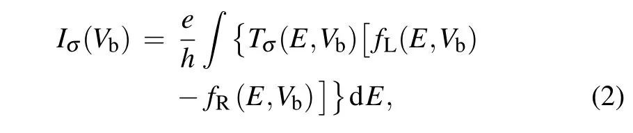
Firstly,we calculate the electronic structures of aAsNRs with N=6,7,8,9,10 as shown in Fig.2.It is found that the spin-up and spin-down bands are split,which means that there appear the magnetic characteristics in all aAsNRs.For N=6 and 7,it is noted that the valence band maximum of spin-up state and the conduction band minimum of spin-down state overlap with Fermi level,thus the spin-metal property can be observed.For N≥8,it is interesting that the valence band maximum of spin-up state gradually approaches the Fermi level at the Γ point with the increase in the width of the nanoribbon.While the conduction band minimum of spindown state turns up,a spin-semiconductor property appears. To explain the mechanism of the spin-dependent band structure of aAsNR,we take N=10 for example.Figures 2(f)and 2(g)show the density of state(DOS)and projected density of state(PDOS)of 10-aAsNR.It is clear that the spin-down DOS peak is above the Fermi energy and several spin-up DOS peaks are below the Fermi level,which corresponds to the two subbands at the Fermi level.According to the PDOS,one can see that the two opposite spin DOS peaks around the Fermi level are determined by the edge atom As1 and its neighboring atom As3.Furthermore,the spin-density distributions at Fermi level for 10-AsNR are shown in Fig.2(h),which are in accordance with the scenario of the PDOS.
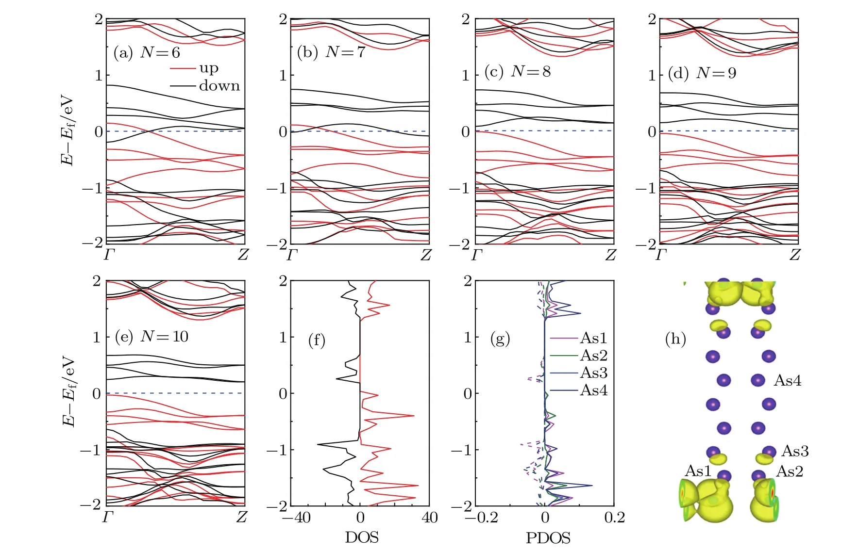
Fig.2.(color online)(a)–(e)Energy band structures of aAsNRs with N=6–10.The zero of energy is set at Fermi level in each system. The red(black)curves represent the spin-up(spin-down)states.(f),(g)DOS and PDOS of 10-aAsNR.(h)Spatial spin distributions (up-down)for the unit cell of 10-aAsNR.The yellow part corresponds to the spin-up electron density greater than the spin-down electron density.
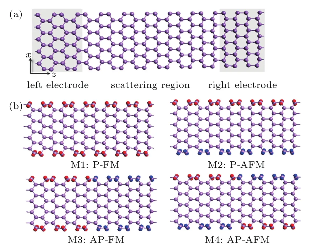
Fig.3.(color online)(a)Device model constructed from aAsNR.(b) Spin density distribution of aAsNR.M1,M2,M3,and M4 refer to the 10-aAsNR under P-FM,P-AMF,AP-FM,and AP-AFM spin configurations,respectively.The red and blue colors refer to the magnetizations M=1 and M=−1,respectively.
We calculate the total energy of the unit cell in spin confi gurations.Our results show that the total energy of the antiferromagnetic(AFM)state is 32.28 meV lower than that of the ferromagnetic(FM)state.The AFM state is the most stable spin configuration.To further explore the magnetic property, we construct a device model based on the aAsNR with N=10 as shown in Fig.3(a).One can control the spin orientations of the electrodes by changing external magnetic field in the two probe system.[26–30]In this work,we consider two types of magnetic configuration.One is a p magnetic configuration, where the right and left electrodes are set to be in the same state by applying a perpendicular external magnetic field,and the other is AP magnetic configuration,where two perpendicular magnetic fields applied externally are antiparallel to two electrodes.Since different spin states have great effects on the graphene nanoribbons[31]and silicon nanoribbons.[32]we also consider the effects of FM and AFM states on the aAsNRs. Therefore,there are four types of magnetic configurations in our calculations exhibited in Fig.3(b),namely,P-FM,P-AFM, AP-FM,and AP-AFM,which are denoted as M1,M2,M3, and M4 for short.For Fig.3(b),we can clearly see that the spin density distribution of the aAsNR is mainly delocalized on the edges of nanoribbons,and well controlled by the magnetic configurations of the electrodes.
Figures 4(a)–4(d)show the variations of current with applied bias voltage(I–V curve)for the four devices M1–M4, respectively.For M1 as shown in Fig.4(a),we can clearly see that the current values of spin-up electrons are always zero in the whole bias range considered.It is different from that of spin-down electrons,when the bias voltage is larger than 1.0 V in the positive bias range,the current of spin-down electrons goes up.In the negative bias voltage range,the spindown current increases when Vb<−1.0 V.Therefore,the device with the P-FM spin configuration favors the identicalspin-directional filtering effect.For the I–V curve of M2 as shown in Fig.4(b),when|Vb|>1.0 V,we can see that both the spin-up and spin-down currents first increase and then drop with increasing bias voltage.In the AP-FM configuration,as the scenario for M3 shows in Fig.4(c),we can also observe that the current is spin-polarized in a very large range of bias [−1.2 V,1.2 V],but it is completely different from the M1 case with P configuration.When|Vb|is lower than 0.8 V, the current is nearly forbidden,and when|Vb|is larger than 0.8 V,the spin-up electrons can pass through the system in negative bias region,while they are still forbidden under positive bias.Furthermore,the spin-down electrons show just the opposite case,they can flow through the system under positive bias and are almost forbidden in the negative bias voltage region.As a result,M3 has a perfect dual spin-filtering effect and dual spin-rectifying behavior,which suggests that the aAsNR-based device with AP-FM spin configuration can act as a dual spin filter or a dual spin diode.For the I–V curve of M4 system as shown in Fig.4(d),in the bias voltage range of [−0.8 V,0.8 V],both spin state currents are nearly forbidden. When the bias voltage is larger than 0.8 V,both currents go up and the current of spin-down rises more quickly than that of spin-up state.While in the negative bias range,the spin-down current goes up more promptly than that of spin-up state.The M4 system also presents the spin splitting phenomenon due to both spin state currents having different trends.
Fig.4.(color online)The I–V curves of 10-aAsNR devices for(a)M1,(b)M2,(c)M3,(d)M4,respectively.The red and black symbols represent the spin-down and spin-up states,respectively.
For the interesting spin splitting phenomena on the I–V curves as shown in Fig.4,we plot spin-filtering efficiency (SFE)in Fig.5.The SFE is often used to comprehend quantitatively the spin-polarization phenomena of the spin devices,which is one of the most important parameter as the spin-filtering function in spin device.The SFE is defined aswhere I↑(I↓)represent the current of spin-up (down)electrons.Figure 5(a)presents the SFE in the negative bias range[−1.2 V,−0.1 V],and figure 5(b)shows the SFE in the positive bias range[0.1 V,1.2 V]for M3.We can find that sizable SFEs can be attained in all bias ranges considered.Especially,the SFEs for M3 in the voltage interval[0.8 V,1.2 V] are large,with a maximum magnitude of 100%.This finding shows that the M3 system we proposed has perfect dual spinfi ltering behavior when the applied bias voltage is larger than 0.8 V.
Furthermore,the dual spin-filtering suggests that M3 has a rectifying effect.One can quantify the rectifying behavior in Fig.4 with the rectifying ratio(R).We can calculate R by using the formula,R=|I(±Vb)|max/|I(±Vb)|min.From Fig.5(c), the rectifying ratio of the spin-up current is very small for the M3 device under lower bias(|Vb|<0.6 V).However,the onset of rectifying effect appears at a bias voltage of 0.6 V,and the spin-up current of M3 exhibits pronounced rectification behavior at a larger bias voltage,and the maximum rectifying ratio can reach 1494 at 0.9 V.Figure 5(d)shows the plot of the rectifying ratio of the spin-down current of M3,and the maximum rectifying ratio is 1297 at 1.0 V.
Comparing the I–V curves of 10-aAsNR based devices for M1–M4 shown in Fig.4,we can clearly see that the I–V curves are significantly affected by the spin configurations of the electrodes.The currents of M3 device in the AP-FM spin configuration are larger than that of the M1 device in the PFM spin configuration.This result suggests that the aAsNRs can act as a giant magnetoresistance device.In order to better understand the giant magnetoresistance.Figures 5(e)and 5(f) present the magnetoresistances(MR)of 10-aAsNR under the FM state in bias ranges of[−1.0 V,−0.1 V]and[0.1 V,1.0 V],respectively.The MR is calculated by using the expression MR=(IAP−IP)/IP,where IAPis the current in the AP(M3) spin configuration and IPis the current in the P(M1)spin configuration.We can clearly find that when the bias is in a bias range of[0.5 V,1.0 V],there are very large MR values for both spin states,and the maximum can even reach 38900000%for spin-down current at a bias of 0.9 V,which is comparable to that of armchair-edged grapheme nanoribbons.[34]

Fig.5.(color online)(a),(b)Spin-filtering efficiencies for M3 device at the negative and positive bias,respectively.(c),(d)Rectifying ratios for the spin-up and spin-down currents of M3 device in a long scale.Arrows↑and↓denote the spin-up and spin-down states. (e),(f)Plots of magnetoresistance versus the applied bias for 10-aAsNR device in a long scale under FM state in the negative and positive bias ranges,respectively.
With a more in-depth understanding of the underlying physics in the interesting spin-filtering effects shown in Figs.5(a)and 5(b),we take M3 configuration for example. The relationships between the electrode band structures and transmission spectra at 1.0 V and−1.0 V and their transmission paths of spin-up and spin-down electrons are shown in Fig.6.The transmission path is an analysis option which splits the transmission coefficient into local bond contributions,Tij. For example,if a system is divided into two parts A and B,the pathways across the boundary between A and B sum up into the total transmission coefficient[35]

The local contribution Tijcan be positive or negative.A positive value means that the electrons flow from siteito site j, while a negative value corresponds to the fact that the electron is back scattered along the bond.According to the transmission spectrum at a bias voltage of 1.0 V shown in Fig.6(a), there are several transmission peaks near the Fermi level for the spin-down electrons;on the contrary,there is no transmission peak but a large zero transmission gap about 1.48 eV near the Fermi level for the spin-up electrons.As the spindependent current at a given voltage is obtained to be the value of T(E,Vb)from Eq.(1),thus the spin-down current outweighs the spin-up current and one observes the perfect spinfiltering effect.From Fig.6(d),we can find that there occur a few transmission peaks near the Fermi level for the spinup electrons,meanwhile a large zero transmission gap appears near the Fermi level for the spin-down electrons at a negative bias of−1.0 V.This means that the spin-up electron is the only one that can pass through the device in the negative bias voltage.This is why we observe a perfect dual spin-filtering effect in the[−1.2 V,1.2 V]bias range.In essence,the spin filtering effect can also be obtained from the band structure of the left and right electrodes and the band structures of both electrodes are in good agreement with the transmission spectra shown in Figs.6(a)and 6(d)for M3.When the bias voltage is positive, the energy band of left electrode shifts downward and upward with respect to that of the right electrode.At a bias of 1.0 V, we notice that the spin-down electrons are preferentially transmitted as both the left and right electrodes have subbands of spin-down electrons in the same bias window.Nevertheless, there is a large band gap for the spin-up electrons of the both electrodes in the same energy range.On the contrary,in the negative bias voltage window,the spin-up subbands of the left and right electrode overlap,and there are only spin-up transmission peaks,while the spin-down transmission value is zero, which means that only the spin-up electrons can path through the left electrode to the right electrode,while the spin-down electrons are forbidden.The transmission path gives a more intuitive explanation.Comparing the transmission paths of spin-up and spin-down electrons under 1.0 eV,we can see that the transmission of spin-down electrons is much stronger than that of spin-up electrons as shown in Figs.6(b)and 6(c),which is in accordance with the I–V curve shown in Fig.4.The transmission pathways can show us the local bond contributions to the transmission coefficient.The transmission paths at−1.0 V are also shown in Figs.6(e)and 6(f).We can see that the spinup electrons can transport through the path,and the spin-down transmission pathway is localized,which is consistent with the I–V curve in Fig.4.As a result,the dual spin-filtering effect and rectifying effect appear on the I–V curves of M3.
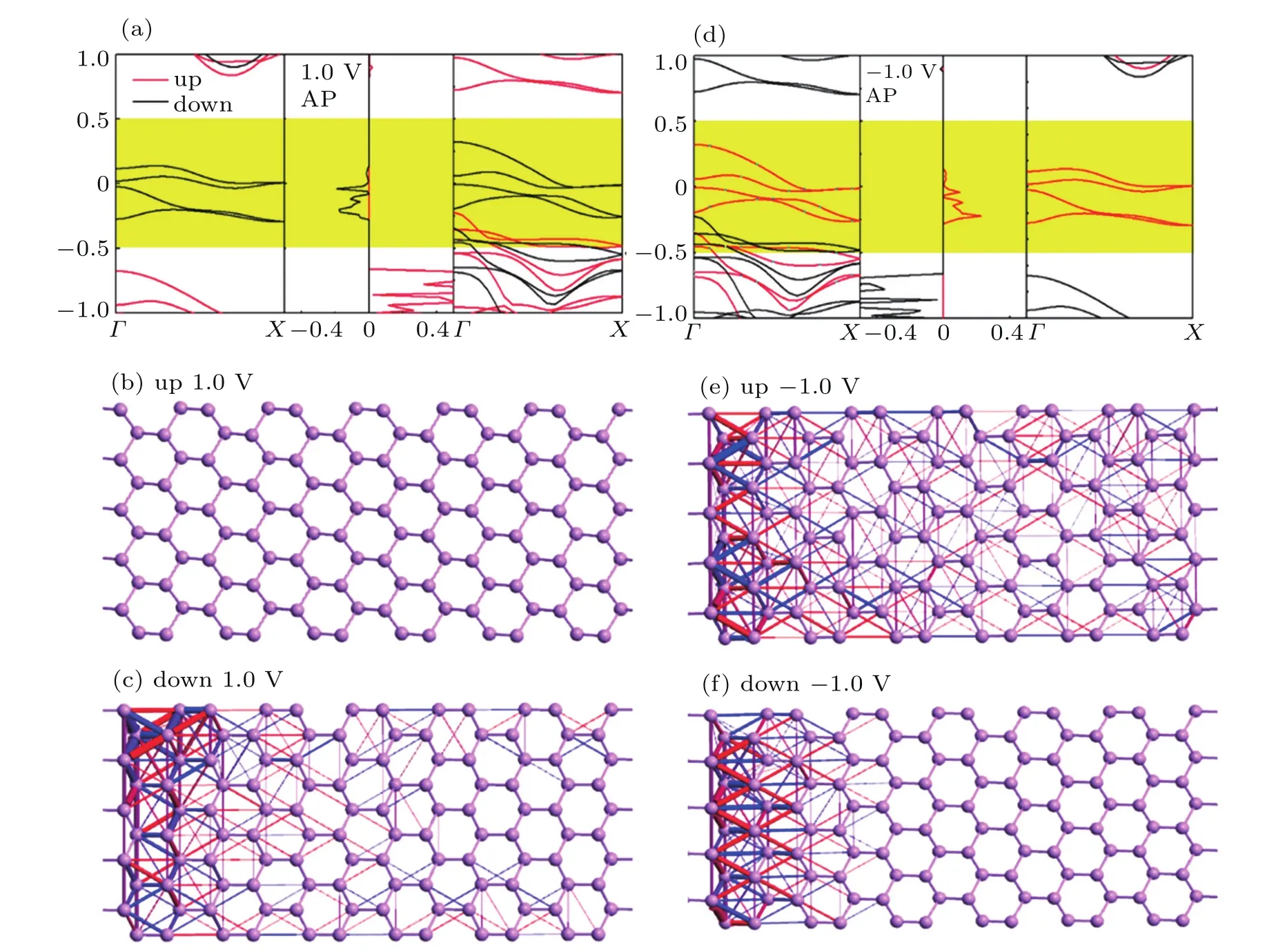
Fig.6.(color online)(a),(d)Left and right panels show the band structures of the left and right electrodes,and the middle panel displays the transmission spectrum of the scattering region for M3 device,correspond to bias of 1.0 V and−1.0 V,respectively.The zero of energy is set at Fermi level.(b),(c)Transmission paths(TPs)of spin-up and spin-down electrons under 1.0 V bias voltage. (e),(f)Transmission paths of spin-up and spin-down electrons under−1.0 V bias voltage,respectively.
4.Conclusions
The spin-dependent transmission properties of aAsNRs are studied by non-equilibrium Green’s function method in conjunction with spin-polarized density-functional theory. Our results show that under the FM magnetic state,for either the P or the AP configuration,the 10-aAsNR system has magnetic property and a certain spin polarization rate.Under the AP-FM configuration,the device shows perfect dual spin-filtering effect with nearly 100%spin polarization and rectifying behavior with maximum rectifying ratios of 1494 for spin-up electrons and 1297 for spin-down electrons,respectively.In particular,significant giant magnetoresistance is found,and the maximum even can reach up to 38900000%. Our research demonstrates that the matching between the band structure of left electrode and that of right electrode plays a key role in determining the spin-dependent transport properties of the aAsNRs-based device.These findings will help to design the high-performance spin functional devices.
[1]Zhang S L,Yan Z,Li Y F,Chen Z F and Zeng H B 2015 Angew.Chem. Int.Ed.54 3112
[2]Zhang S L,Hu Y H,Hu Z Y,Cai B and Zeng H B 2015 Appl.Phys. Lett.107 022102
[3]Kou L Z,Ma Y D,Tan X,Frauenheim T,Du A and Smith S 2015 J. Phys.Chem.C 119 6918
[4]Kamal C and Ezawa M 2015 Phys.Rev.B 91 05423
[5]Wang Y and Ding Y 2015 J.Phys.:Condens.Matter 27 225304
[6]Majid Z,Mehdi S,Sarsari I,Pourfath M and Donadio D 2016 Phys. Rev.B 93 085424
[7]Zhang S L,Xie X Q,Li F Y,Li Z Y,Kan E,Liu W,Chen Z F and Zeng H B 2015 Angew.Chem.Int.Ed.55 1666
[8]Zhang Z Y,Xie J F,Yang D Z,Si M S and Xue D S 2014 Appl.Phys. Express 8 055201
[9]Han J W,Xie J F,Zhang Z Y,Yang D Z,Si M S and Xue D S 2015 Appl.Phys.Express 8 4
[10]Norman N C 1998 Chemistry of Arsenic,Antimony,and Bismuth (Springer Scienceamp;Business Media)
[11]Zhu Z,Guan J and Tomanek D 2015 Phys.Rev.B 91 161404
[12]Cao H,Yu Z and Lu P 2015 Superlattice Microst.86 501
[13]Wang Y P,Zhang C W,Ji W X,Zhang R W,Li P,Wang P J,Ren M J, Chen X L and Yuan M 2016 J.Phys.D:Appl.Phys.49 055305
[14]Wang Y P,Ji W X,Zhang C W,Li P,Ren M J,Chen X L,Yuan M and Wang P J 2015 Sci.Rep.6 20342
[15]Zhang H,Ma Y and Chen Z 2015 Nanoscale 7 19152
[16]Wang C,Xia Q,Nie Y Z and Guo G H 2016 AIP Advances 6 035204
[17]Du J,Xia C X,An Y P,Wang T X and Jia Y 2016 J.Mater.Sci.51 9504
[18]Wang Y P,Zhang C W,Ji W X and Wang P J 2015 Appl.Phys.Express 8 065202
[19]Li Z J,Xu W,Yu Y Q,Du H Y,Zhen K,Wang J,Luo L B,Qiu H L and Yang X B 2016 J.Mater.Chem.C 4 362
[20]Tsai H S,Wang S W,Hsiao C H,Chen C W,Yang H O,Chueh Y L, Kuo H C and Liang J H 2016 Chem.Mater.28 425
[21]Zhang Z Y,Xie J F,Yang D Z,Wang Y H,Xue D S and Si M S 2014 Eprint Arxiv.8
[22]Wang Y and Ding Y 2015 Nanoscale Res.Lett.10 955
[23]Taylor J,Guo H and Wang J 2001 Phys.Rev.B 63 245407
[24]Perdew J P and Zunger A 1981 Phys.Rev.B 23 5048
[25]Buttiker M,Imry Y,Landouer R and Pinhas S 1985 Phys.Rev.B 31 6207
[26]Kim W Y and Kim K S 2008 Nat.Nanotech.3 408
[27]Li M J,Zhang D,Gao Y L,Cao C and Long M Q 2017 Org.Electron. 44 168
[28]Zhang D,Long M Q,Zhang X J,Ouyang F P and Li M J 2015 J.Appl. Phys.117 014311
[29]Li X M,Long M Q,Cui L L,Xiao J,Zhang X J,Zhang D and Xu H 2014 Phys.Lett.A 378 2701
[30]Li X M,Long M Q,Cui L L,Xiao J and Xu H 2014 Chin.Phys.B 23 047307
[31]Cui L L,Long M Q,Zhang X J,Li X M,Zhang D and Yang B C 2016 Phys.Lett.A 380 730
[32]Zhang D,Long M Q,Zhang X J,Cao C,Xu H,Li M J and Chen K S 2014 Chem.Phys.Lett.616 178
[33]An L P and Liu N H 2012 New Carbon Mater 27 181
[34]Zhu Z,Li C X,Zhang Z H 2016 Acta Phys.Sin.65 118501(in Chinese)
[35]Solomon G C,Herrmann C,Hansen T,Mujica V and Ratner A 2010 Nat.Chem.2 223
20 March 2017;revised manuscript
6 June 2017;published online 31 July 2017)
10.1088/1674-1056/26/9/098509
∗Project supported by the National Natural Science Foundation of China(Grant Nos.21673296 and 11334014),the Science and Technology Plan of Hunan Province,China(Grant No.2015RS4002),and the Postdoctoral Science Foundation of Central South University,China.
†Corresponding author.E-mail:limingjun@csu.edu.cn
‡Corresponding author.E-mail:mqlong@csu.edu.cn
©2017 Chinese Physical Society and IOP Publishing Ltd http://iopscience.iop.org/cpb http://cpb.iphy.ac.cn
猜你喜欢
小猕猴智力画刊(2021年10期)2021-04-21
方圆(2017年1期)2017-02-13
师道(2016年5期)2016-05-14
小小说月刊·下半月(2014年4期)2014-05-14
作文大王·语林(2013年12期)2013-12-30
为了孩子(孕0~3岁)(2009年19期)2009-11-30
小小说月刊(2009年8期)2009-11-22
语文天地·初中版(2009年6期)2009-07-22
小小说月刊(2008年3期)2008-03-03
青年文摘·上半月(1991年7期)1991-01-01

- Chinese Physics B的其它文章
- Improved control for distributed parameter systems with time-dependent spatial domains utilizing mobile sensor actuator networks∗
- Geometry and thermodynamics of smeared Reissner–Nordström black holes in d-dimensional AdS spacetime
- Stochastic responses of tumor immune system with periodic treatment∗
- Invariants-based shortcuts for fast generating Greenberger-Horne-Zeilinger state among three superconducting qubits∗
- Cancelable remote quantum fingerprint templates protection scheme∗
- A high-fidelity memory scheme for quantum data buses∗