
A terahertz on-chip InP-based power combiner designed using coupled-grounded coplanar waveguide lines∗
2021-12-22 06:42HualiZhu朱华利YongZhang张勇KunQu屈坤HaomiaoWei魏浩淼YukunLi黎雨坤YuehangXu徐跃杭andRuiminXu徐锐敏
Chinese Physics B 2021年12期
关键词:张勇
Huali Zhu(朱华利), Yong Zhang(张勇), Kun Qu(屈坤), Haomiao Wei(魏浩淼),Yukun Li(黎雨坤), Yuehang Xu(徐跃杭), and Ruimin Xu(徐锐敏)
School of Electronic Science and Engineering,University of Electronic Science and Technology of China,Chengdu 611731,China
Keywords: coupled-GCPW, InP technology, terahertz monolithic integrated circuits (TMICs), Wilkinson power combiner
1. Introduction
In recent years, terahertz monolithic integrated circuits(TMICs) have been developing rapidly and gaining attention due to advancements in transistor technologies, such as InP heterojunction bipolar transistors. The potential application areas for TMICs include high-speed wireless communication,wireless sensing, spectroscopy, and imaging.[1–3]The power combiners, such as Wilkinson combiners,[4–6]Tee-junction combiners,[7,8]Dolph–Chebyshev combiners,[9–11]and integrated planar spatial combiners,[12]are the essential and vital components,which increase the output power of the terahertz devices.
Owing to their excellent port isolation performance and low-loss, the Wilkinson combiners are most commonly used in power amplifiers. However, as depicted in Fig. 1(a), the coverage area is relatively large due to the two unavoidable quarter-wavelength transmission lines and isolation resistor.In order to achieve length reduction in the quarter-waveguide transmission lines, many technologies have been proposed in the millimeter-wave band, such as capacitive and inductive loading[13]and elevated coplanar waveguide (CPW).[14]Unfortunately, for the combiners operating at terahertz frequencies, using the above technologies significantly deteriorates the performance of the Wilkinson combiners due to the parasitic parameter induced by the additional structure.[15]
Grounded coplanar waveguide (GCPW) as the main transmission lines has been commonly used in designs of numerous TMICs due to its superior characteristics, including small dispersion, easy integration with lumped elements as well as active components, and great heat dissipation.Nonetheless, the Wilkinson combiner based on GCPW lines operating in the terahertz range is rare due to the complexity of the isolation resistor layout and the narrowband features.
In order to resolve the above-discussed problem,a novel terahertz power combiner using coupled-GCPW Wilkinson combiner is proposed in this article. Apart from the conventional designs,as depicted in Fig.1(b),the quarter-wavelength GCPW lines are substituted with the coupled-GCPW lines and located at the end of the input port.The use of coupled-GCPW lines in realizing the inevitable quarter-wavelength sections can cause the coverage area minimization of the Wilkinson combiner.[16,17]In order to demonstrate the proposed topology, a two-way back-to-back combiner and a four-way backto-back combiner, operating in a 210–250 GHz frequency range and based on a 50-µm-thick InP TMICs process were designed,fabricated,and measured.
2. Design of the proposed power combiner
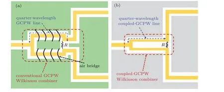
Fig.1. The schematic diagram of the Wilkinson combiners. (a)Conventional GCPW Wilkinson combiner. (b)Coupled-GCPW Wilkinson combiner.
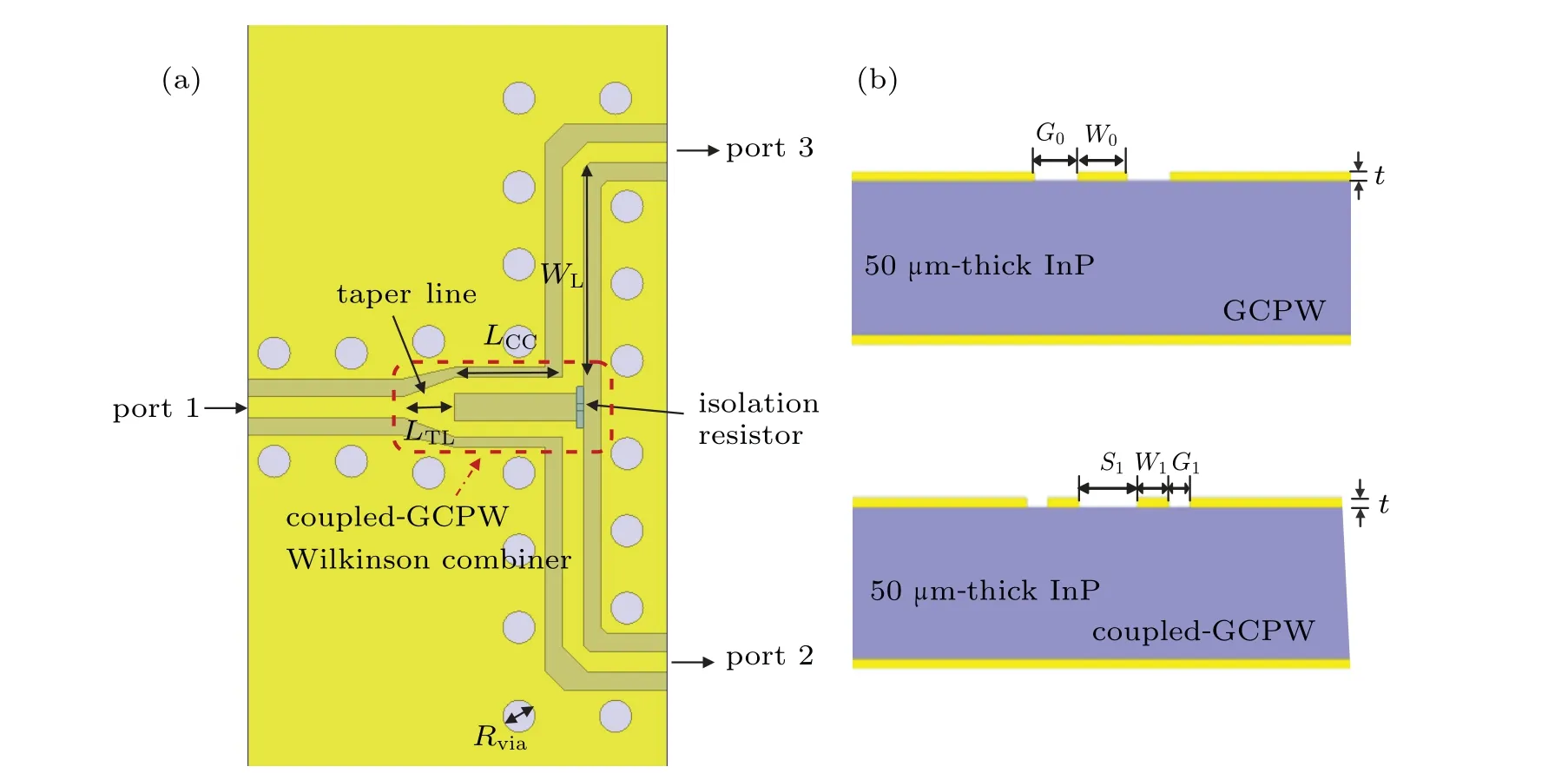
Fig.2. The three-dimensional views of the proposed coupled-GCPW combiner: (a)front view of the per combiner,(b)a cross-sectional view of the GCPW transmission line and the coupled-GCPW transmission line. (LTL=40µm,W =16µm,G=14µm,W1=12µm,G1=8µm,S1=22µm,WL=200µm,Rvia=25µm,t=3µm).
Figure 2(a)shows the three-dimensional view of the proposed combiner, and the topology consists of a GCPW input port, two GCPW output ports, and a coupled-GCPW Wilkinson combiner.Two coupled-GCPW lines at the end of port 1 of the Wilkinson combiner is the replacement of the two quarterwavelength GCPW lines, where the input and output ports are standard GCPW lines with the characteristic impedance of 50 Ω. Additionally,the isolation resistor was determined to be 100 Ω to ensure high isolation characteristics and equal power ratios between port 2 and port 3.The two GCPW lines with the length ofWLadded between the coupled-GCPW Wilkinson combiner and the output ports facilitate lateral widths adaption of the power combiner chip.
The use of coupled-GCPW as the quarter-wavelength transmission lines provides two advantages over the conventional Wilkinson power combiner. Firstly,placing the ground pads of the two coupled-GCPW lines outside the combiner can overcome the air bridge interconnects of the inner ground pad in the conventional Wilkinson power combiner. Secondly,the reduction in the Wilkinson combiner coverage area in the designed chip aids in fulfilling the electrical performance requirements, thereby achieving possible miniaturization and maintaining a low cost. As there is no special module for the coupled-GCPW structure calculations, formula-based approximate size calculations are performed initially. Later,the HFSS software performs separate simulations for the coupled-GCPW structure to determine the impedance that meets the design requirements. Lastly,to obtain the optimal value of the overall coupled-GCPW structure,adjustments are made.
The principle of the conventional Wilkinson combiner is the basis for the coupled-GCPW Wilkinson combiner, which can be easily analyzed using even-mode and odd-mode excitations of port 2 and port 3 with a loadZ0connected to port 1.[16]The even-mode excitation of the design is symmetrical,having symmetry in the field distribution of the two coupled-GCPW lines and the symmetry plane of the coupled-GCPW equivalent to an open circuit. The odd-mode excitation of the design is asymmetrical,with equal and inverting field distribution in the two coupled-GCPW lines,and the symmetry plane of the coupled-GCPW equivalent to a short circuit. The operation bandwidth is a ratio of the even-modeZeand odd-modeZo,and the broadest bandwidth is at the ratio value equal to 1.As shown in Fig.2(b),the geometrical parameters of GCPW,G0andW0, are calculated according to the 50 Ω characteristic impedance. Moreover, the initial values of the coupled-GCPW,Ze/Zo/W1/G1/S1can be calculated by the analytical formulation of the quasi-static even-and odd-mode characteristics of the coplanar coupled lines,as described in the previous studies:[18]

whereK(t(o,e))andK′(t(o,e))are the complete elliptic integral of the first kind and its complement,respectively,with the precise expressions reported in an earlier study.[19]Thef(o,e)is a function ofεrand the substrate thickness, which have been discussed further in earlier studies.[18]The mode impedances ofZeandZoobtained from these calculations were 72 Ω and 45 Ω,respectively.
Using the above-stated values,a simulated structure of the proposed combiner was established with the considerations of the design rules of the 50-µm-thick InP process. The fullwave simulator simulates and optimizes the practical circuit,and the isolation resistor is an ideal high resistive region with ideal contacts.
In order to better understand the proposed combiner principle, we further studied the general effect of the coupled-GCPW lengths(LCC)and the lateral width(WL). As depicted in Fig.3(a),theS-parameters for differentLCCwere simulated to demonstrate the relationship between the center frequency andLCC. It was established that theLCCdirectly impacts the central frequency of the combiner,with the peak of return lossS11continually moving from the frequency region of 250 GHz to 210 GHz and maintaining similar operating bandwidth, as theLCCincreases from 60 µm to 80 µm. AtLCC=75 µm,the peak ofS11is around 220 GHz, with an improved lowloss characteristic. At 220 GHz, for the quarter-wavelength line of the Wilkinson combiner, the theoretical length should be 98 µm, which is a deviation from the simulated coupled-GCPW line length. It is revealed that as the above theoretical calculation method is based on the ideal even- and oddmode analysis characteristics, the final size selection must be according to the full-wave simulator.Figure 3(b)depicts theSparameters according to the lateral width(WL). The proposed coupled-GCPW Wilkinson combiner has uniform broadband and low-loss characteristics for the frequency region of 210–250 GHz,withWLincreasing from 100µm to 300µm. Thus,it is confirmed that the proposed structure is appropriate for terahertz chips with different lateral widths.
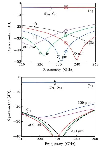
Fig. 3. Simulated S-parameters of the proposed combiner. (a) Simulated S-parameters as a function of the length of coupled-GCPW(LCC).(b)Simulated S-parameters as a function of the lateral width(WL).

Fig.4. The electric field distribution at 220 GHz of the proposed combiner based on the coupled-GCPW.
In addition, the line widthW1and the spacingS1can be adjusted and optimized to obtain equal output signals and low insertion losses at ports 2 and 3. A tapered line is added to improve the matched-degree between the standard GCPW and the coupled-GCPW,while the cutting corners in ports 2 and 3 reduce the mismatch at transmission line discontinuities.
According to the optimized geometrical parameters, as shown in Fig.4, the electric field distribution at 220 GHz for a two-way back-to-back combiner was simulated. The input electric field energy fed to port 1 propagates through the standard GCPW and converts to an even mode of the coupled-GCPW.[16]Propagation through the coupled-GCPW forms two components with phase congruence occurring at ports 2 and 3. Subsequently,a back-to-back combiner is formed by a symmetrical structure design.
3. Results and discussion
Figure 5 shows theS-parameter measurements of the proposed power combiner chip by the on-wafer probe using an Agilent N5247A VNA with 220–325 GHz frequency-extender modules. In order to ensure the reference planes on the probe tips, the line-reflect-reflect-match (LRRM) on-wafer calibration was applied.
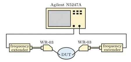
Fig.5. Test setup for S-parameters measurements.
Figure 6 presents a micrograph of the fabricated two-way back-to-back combiner based on an Au surface micromachining process on the 50-µm-thick InP substrate,with the overall chip dimension of 650µm×650µm. The vector network analyzer can measure the combiner,with two additional GCPW pads added to the input and the output ports. Simultaneously,to verify that the structure has excellent characteristics during multi-combining, a four-way back-to-back combiner was fabricated using the same technologies. Figure 7 depicts a micrograph that occupies a die size of 1250µm×750µm. The geometry and the isolation resistors of the two coupled-GCPW Wilkinson combiners are the same. The metal layer covering the ground in the chips causes the vias no-visibility on the micrographs.
Figures 6 and 7 show the insertion lossS21and the return lossS11,respectively,for the combiners. According to the results, for the frequency range of 210–250 GHz, the insertion losses of the two-way back-to-back combiner and four-way back-to-back combiner were lower than 2.1 dB and 2.7 dB,respectively.In addition,the return losses were lower than 11 dB in the frequency region. It translates to a loss per two-way combiner and a four-way combiner of 1.05 dB and 1.35 dB,respectively. In comparison,the insertion losses were in good agreement with the simulated ones,and the return losses deteriorated within an acceptable limit. To the best of our knowledge,with the rise in the frequency to the terahertz band,complicated parasitic effects induced by the on-wafer probe become difficult to ignore. In addition,the errors occurring during processing in the subtle structures are inevitable, such as the assumption of vias metallization, the inaccuracy of modeling of isolation resistors. The above factors will cause the returning loss to deteriorate.

Fig.6. Simulated(solid line)and measured(dashed line)S-parameters for the two-way back-to-back combiner.
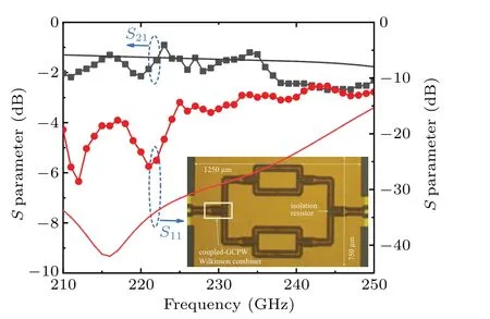
Fig.7. Simulated(solid line)and measured(dashed line)S-parameters for the four-way back-to-back combiner.
It is worth mentioning that the measured losses of the proposed combiners include the loss of RF pads and standard GCPW lines. As for the standard, long GCPW lines were designed, in the middle of the combiner, to ensure enough space for the amplifier circuit, i.e., 500 µm for a two-way back-to-back combiner and 800 µm for a four-way back-toback combiner. Thus,it was inferred that the actual losses of the coupled-GCPW Wilkinson combiners were lower than the measured ones.
In order to demonstrate the excellent performance of the proposed coupled-GCPW Wilkinson combiner, Table 1 presents the comparative analysis with the other state-of-theart terahertz power combiners operating above 100 GHz. The per-cell combiner size considered in this study excludes the RF pads,input and output lines,and reserved space for the amplifier circuit.Small-size and low-loss have been shown in earlier studies,[4,12]respectively,and the transmission lines of the two combiners are microstrip, which is noteworthy. When compared with the microstrip technology,the transmission line of GCPW has lower dispersion and better heat dissipation performance, which is more suitable for the terahertz devices.As compared to the GCPW-based Wilkinson power combiners presented in earlier studies,[5,6]the structure proposed in this paper significantly reduces the insertion loss and the combiner size. Compared to the GCPW-based combiner presented in earlier studies,[10]the proposed combiner presents improved broadband features while maintaining the other superior performance parameters.
The results evidenced that, compared to other GCPWbased Wilkinson combiner, the design proposed in this study substantially improves the performance by lowering the combiner size and insertion loss by nearly two times of those presented by the others. To the best of the knowledge, among the terahertz InP GCPW-based Wilkinson combiners,the proposed design presents the smallest losses along with excellent broadband performance and smaller size. Thus, the overall property of the proposed combiner design is superior, which makes it versatile.
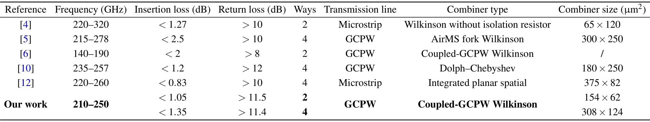
Table 1. Comparison of the state-of-the-art integrated power combiners above 100 GHz.
4. Conclusion
This paper describes an on-chip power combiner based on the coupled-GCPW Wilkinson combiner operating in the terahertz range. Two coupled-GCPW lines were used to substitute the two inevitable quarter-wavelength GCPW lines,which have greatly resolved the complex layout problem of the terahertz on-chip Wilkinson combiners. A two-way back-to-back combiner and a four-way back-to-back combiner were fabricated on the 50-µm-thick InP substrate and measured by the on-wafer probe using an Agilent N5247A VNA with frequency extender modules. The power combiner proposed in this work has lower insertion losses,compact size,and stable broadband performance and is, therefore, versatile for many terahertz devices such as power amplifiers and signal distribution networks.
猜你喜欢
Chinese Physics B(2022年11期)2022-11-21
Chinese Physics B(2022年7期)2022-08-01
Chinese Physics B(2022年7期)2022-08-01
做人与处世(2022年6期)2022-05-26
做人与处世(2022年4期)2022-05-26
科技风(2022年7期)2022-03-15
书香两岸(2020年3期)2020-06-29
现代临床医学(2019年6期)2019-12-07
小猕猴学习画刊·下半月(2019年8期)2019-09-16
理科考试研究·初中(2017年4期)2017-11-04
- Chinese Physics B的其它文章
- Transient transition behaviors of fractional-order simplest chaotic circuit with bi-stable locally-active memristor and its ARM-based implementation
- Modeling and dynamics of double Hindmarsh–Rose neuron with memristor-based magnetic coupling and time delay∗
- Cascade discrete memristive maps for enhancing chaos∗
- A review on the design of ternary logic circuits∗
- Extended phase diagram of La1−xCaxMnO3 by interfacial engineering∗
- A double quantum dot defined by top gates in a single crystalline InSb nanosheet∗