
Strategy to mitigate single event upset in 14-nm CMOS bulk FinFET technology
2022-05-16 07:10DongQingLi李东青TianQiLiu刘天奇PeiXiongZhao赵培雄ZhenYuWu吴振宇TieShanWang王铁山andJieLiu刘杰
Chinese Physics B 2022年5期
Dong-Qing Li(李东青) Tian-Qi Liu(刘天奇) Pei-Xiong Zhao(赵培雄)Zhen-Yu Wu(吴振宇) Tie-Shan Wang(王铁山) and Jie Liu(刘杰)
1Institute of Modern Physics,Chinese Academy of Sciences,Lanzhou 730000,China
2University of Chinese Academy of Sciences,Beijing 100049,China
3School of Physical Science and Technology,Lanzhou University,Lanzhou 730000,China
4National University of Defense Technology,Changsha 410000,China
5Tsinghua University,Beijing 100084,China
Keywords: TCAD simulation,FinFET,single event upset(SEU)mitigation
1. Introduction
Dual-interlock cell (DICE) design has been widely used in hardened static random-access memory(SRAM)devices to reduce the occurrence of single event upset (SEU) in space environment. In theory, the SEU can be eliminated when only one sensitive node is affected in an SRAM cell with DICE design.[1]With the development of digital integrated circuits, the integration increases strongly, which causes the distance between sensitive nodes to decrease in DICE. Under the action of charge sharing, charge collection can occur in multiple nodes simultaneously, which weakens the protection of DICE from the SEU.[2—4]In sub-100-nm technology,the DICE becomes vulnerable to the SEU.[5,6]For a 40-nm bulk technology node, the effects of DICE design on proton and neutron single-event are negligible.[7]Accordingly, dual DICE interleaving design which can increase the distance between the sensitive nodes in DICE was proposed as a feasible solution.[8,9]For a commercial 65-nm CMOS technology,the dual DICE interleaving cells show about 2—3 orders of magnitude lower in SEU cross sections than the 6T-SRAM cells due to the 2-μm nodal spacing of sensitive pairs,[5]for which the charge sharing between devices is significantly reduced.[10]However, taking 22-nm SOI FinFET device for example, the width of an SRAM cell is about 0.2 μm,[11]which means the 0.4-μm nodal spacing even for an interleaving DICE. Therefore,for sub-22-nm technology,especially for FinFET device,which has higher integration than the planar device, we infer that the protection of dual DICE interleaving from SEU will also be greatly weakened.
On the other hand,radiation hardened by design(RHBD)for single event transient (SET) mitigation has been widely studied. Many methods have been proposed, such as source extension,[12]high density well contact (HDWC),[13]pulse quenching layout,[14]and NMOS location adjustment.[15]
Although the SET width is closely related to the SEU,these methods are rarely applied to SEU mitigation. Probably,the main reason is not so effective than the DICE or the triple modular redundancy(TMR).[16]The source extension design in the 65-nm technology sets up 25% area of dissipation and reduces 19.0%of SET pulse width for heavy ion with an LET value of 32.5 MeV·cm2/mg.[12]The pulse quenching layout can be applied only to the logic gates with multiple stages.[17]For the NMOS transistor location adjustment technology, at the minimum distance (160 nm) between NMOS transistor and N-well, the average SET pulse width of 65-nm inverter can be reduced to 18.6%for Ge ion irradiation,while the SET map has not been significantly changed compared withthe SET mapof the maximum distance.[15]In particular, solid guard rings or intermittent rings are used in DICE to prevent the single event latchup(SEL)and charge sharing to occur,[8]which also inhibits the bipolar amplification of PMOS,so are they in HDWC.
In consideration of the increased integration with scaling down, for example, in 22-nm bulk FinFET, the distance between NMOS and N-well decreases to about 40 nm,[18]which will enhance the absorption capacity of N-well to electrons around off-NMOS drain and the restoring current of PMOS.[15]Therefore, we think that the NMOS transistor location adjustment design to mitigate single event response becomes more effective. On the other hand, in sub-22-nm technology node,keeping the nodal spacing between sensitive nodes of DICE increasing to 2 μm is hard and will lead the power dissipation to increase, and speed to decrease and the topology to turn complex. Therefore, the influence of MOSFET locations on SEU cross section of advanced SRAM cell deserves to be further studied.
In this work,through mixed-mode 3D-TCAD simulation,the influences of NMOS location and PMOS location on SEU cross section are analyzed. The effect of reducing the distance between PMOS and P-substrate on SET pulse width has not been studied,[15]because the results[19]demonstrated that the distance between PMOS and N-well tap should be minimum for P-hit SET mitigation. Considering this problem can be addressed by adding N-well tap or adjusting the tap location, the influence of PMOS location is also studied in our simulation. The result shows that the SEU cross sections of PMOS and NMOS decrease significantly by reducing the distance between well boundary and metal—oxide—semiconductor field-effect transistors(MOSFETs).Besides,by enhancing the stabilizing effect of taps on N-well and P-substrates,the inhibition effect of MOSFET location adjustment on SEU is more significant for higher LET ion irradiations. Furthermore, the feasibility of this method is also discussed in detail.
2. Simulation setup
2.1. Principle
When ions pass through static random-access memory(SRAM),electron—hole pairs are generated along the ion trajectories. The off-NMOS(NMOS2)and off-PMOS(PMOS1)are both sensitive nodes of SRAM cell as shown in Fig.1(a).
Taking the off-NMOS for example, after electron—hole pairs are generated,the drain collects deposited electrons,resulting in SEU. At the same time, the built-in electric field at the N-well boundary also absorbs the deposited electrons to N-well, competing with the off-NMOS drain as shown in Fig. 1(b). Besides, the deposited electrons in N-well causes the electrostatic potential to decrease,triggering the bipolar effect of PMOS and generating restore current in the on-PMOS drain.[15]
For the off-PMOS, the physical process is similar, except that the collected charge is hole and the bipolar effect of NMOS is weaker due to the structure of P-substrate.[12]

Fig. 1. Schematic diagram of (a) SRAM cell and (b) competition between off-NMOS drain and well boundary.
2.2. Distribution of incident ions
The charge collection and single-event response will be affected by ionization track structure[20,21]while the normalized distribution of ion track is determined mainly by the ion energy (MeV/amu).[22]To avoid the influence of normalized distribution and ensure the accuracy of the simulation, the structure of 10-MeV/amu krypton is set as the input model(see Fig.2)in TCAD simulation,based on Geant4 simulation result of related investigation.[23]
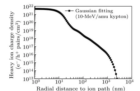
Fig. 2. Gaussian fitting of ion track structure[23] for krypton ion from 10-MeV/amu cocktails. The charge distributions of different LET ions can be achieved by multiplying the structure by LET/LETKr.
The fitting formula of normalized distribution is shown as follows:

withA1—A7being 0.01, 0.02, 0.03, 0.03, 0.05, 0.08, 0.076;W1—W7being 900,600,280,140,56,18,14(in unit nm).
2.3. TCAD model simplification and calibration
The SET in two interlocking inverters determines whether the SRAM cell is upset. Therefore,to save computational resources,the two NMOS transistors only for“read”and“write”are omitted in our simulation.
The 3D-TCAD mixed models are built up using Sentaurus TCAD simulator. Referring to the predictive technology model (PTM) from Arizona State University[24]and 14-nm FinFET model document,[25]the channel length,the fin width at top and those at bottom are 15 nm, 10 nm, and 40 nm,respectively. For the high-kgate dielectric, two monolayers of SiO2interlayer (6 °A) and HfO2(17 °A) are built. TheId—Vgcurves of NMOS and PMOS are and theId—Vgcurves of 14/16-nm planar devices are calibrated by LT-Spice simulator,referring to Ref. [26]. Besides, in consideration of the better grid control-ability in FinFET on subthreshold slope,the curve(see Fig.3)is adjusted to 15-nm FinFETId—Vgcharacteristics in Ref. [27]. It was demonstrated in Ref. [28] that the influence of inverter transient switching time on single-event effect cannot be ignored. Therefore, the switching time in our simulation is calibrated to be less than 1 ps,[29]ensuring that the SRAM cell is sensitive to small LET ions. The bias dependence of SEU cross section calculated by this TCAD model is consistent with the experiment result in Ref.[30].

Fig. 3. Characteristic curve of drain current versus gate voltage of 3DTCAD 16-nm NMOS model with 0.1-V source—drain voltage.
2.4. Simulation process
The layout diagram of simulation model is illustrated in Fig. 4. Figure 4(a) shows the high integration of transistors under the influence of the N-well boundary and adjacent transistors. Referring to Refs. [11,31] the width of N-well and P-substrate are set to be 200 nm. The distance of NMOS and PMOS to N-well boundary are bothLM. By adjustingLM,the influence of MOSFET location on SEU map is analyzed. Figure 4(b) acts as a contrast to analyze the SEU map without the influence of well boundaries. The PMOS and NMOS are located in the center of N-well and P-substrate respectively,which are both 3 μm in width,ensuring that the transistors are almost unaffected by N-well boundary and the restoring current in the same inverter. By comparing the SEU maps under layouts of Figs.4(a)and 4(b),the influence of well boundaries and restoring current on SEU cross section can be presented.Besides, it can help distinguish between the sensitive points belonging to off-NMOS drain and off-PMOS drain in the SEU maps under the layouts of Fig.4(a).

Fig.4. (a)In consideration of the effect of well boundary and adjacent transistors on SEU cross section and (b) their contrast (pull away the distance between the boundary and the transistor to 1.5 μm). For clarity, shallow trench isolation(STI)layer and polysilicon are removed. LT represents the distance between taps and the center of off-NMOS drain. Taps are located on both sides of the off-NMOS.
The SEU maps are obtained by normal incident ions located around the sensitive transistors. The sum of areas where the incident ions pass and cause the SEU is the cross section.
3. Results and analysis
3.1. SEU mitigation of different LET ion irradiations
The SEU maps are shown in Fig. 4(a) with 0.8-μmLTand 40-nmLMand Fig.4(b)to prove that well boundary and the restoring current affect the SEU cross section.Besides,the changes of inhibition degree on SEU cross section with different LET ion irradiations are studied as shown in Fig. 5 and Table 1.

Fig. 5. SEU map of (a) NMOS and (b) PMOS with well boundary pulled away. (c)SEU map of SRAM cell.

Table 1. SEU cross section ratio(σ40/σb)with LET.
As illustrated in Table 1, the SEU cross section ratio of NMOS is smaller than that of PMOS under the same LET,and decreases with LET for both NMOS and PMOS except for NMOS under the irradiation of heavy ion with LET of 33.2 MeV·cm2/mg.
The reason is that the larger cross section is affected seriously by well boundary, because the well boundary passes through the cross section more internally. As shown in Fig.5,the cross section in higher LET ion irradiation is larger,and the cross section of NMOS is larger than that of PMOS.The cross section of NMOS and PMOS are contrast to that in Ref.[31],where the pulse widths of P-hit SETs are larger than those of N-hit. For the 65-nm inverter in Ref.[32],the area of PMOS is larger than that of NMOS and its parasitic-bipolar effect is more significant PMOS’s, while for FinFET devices, PMOS area is the same as NMOS area. Besides, the hole mobility is much smaller than electron mobility, causing the collected charge of off-PMOS drain to be reduced by more serious recombination (see in Fig. 6). A similar situation is found in Ref. [33], for the 65-nm bulk CMOS technology, in normal incident ion with low LET,the pulse widths due to P-hits are smaller than due to N-hits.
For the NMOS SEU cross section of ions with LET of 33.2 MeV·cm2/mg,we suppose that the abnormal behavior is caused by the excess deposited electrons,which is hard to control by well boundary and taps. This part is analyzed in Subsection 3.3.
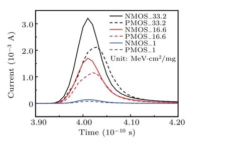
Fig.6. Current pulses of single off MOSFET.Normal incident ions are located at the drain centers.
3.2. Influence of distance between MOSFET and well boundary
The SEU maps of SRAM cell, respectively, withLMof 60 nm, 40 nm, 20 nm under the ion irradiation of 33.2 MeV·cm2/mg, 16.6 MeV·cm2/mg, 1 MeV·cm2/mg are shown in Fig.7. The decreasing trends of SEU cross sections withLMincreasing is illustrated as shown in Fig.8.
3.2.1. Electric potential distribution in well boundary
It is shown that the SEU cross sections decrease faster with the decrease ofLM, and the trends of cross sections decreasing withLMbecome more significant with LET increasing for both PMOS and NMOS except for the NMOS in the ion irradiation of 33.2 MeV·cm2/mg. This is because of the non-uniformity of well boundary electric field and bipolar effect of PMOS. As shown in Fig. 9, when the sensitive node center approaches to the well boundary, the electric potential in cross section increases faster and faster,resulting in the accelerating of cross section decreasing withLMincreasing and the influence of large cross section greater than that of small cross section due to being closer to well boundary. The reason for the abnormal situation of NMOS in 33.2 MeV·cm2/mg ion irradiation is similar to that in Subsection 3.1.
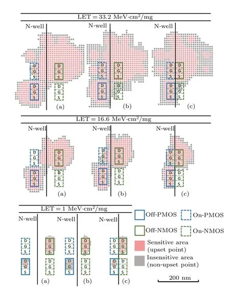
Fig.7. SEU maps of SRAM cells with LM of(a)60 nm,(b)40 nm,and(c)20 nm.

Fig.8. Variation trends of SEU cross section ratio with LM in different LET ion irradiations, with A(60) denoting SEU cross section of SRAM with LM of 60 nm.
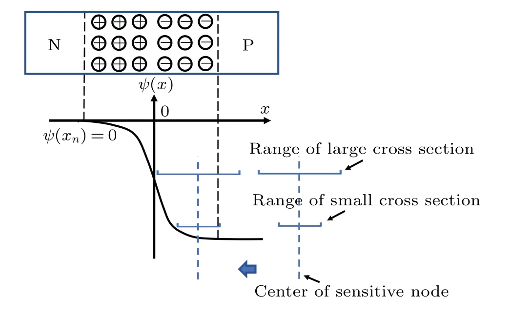
Fig.9. Current pulses of single off MOSFET.
3.2.2. Bipolar effect of PMOS
As shown in Fig.8,for the same LET,the SEU cross section of PMOS decreases faster than that of NMOS.To explain this phenomenon, in consideration of the fact that the bipolar amplification effect can significantly improve the SEU sensitivity of PMOS and the bipolar effect of NMOS is not obvious in NMOS due to the structure of P-substrate,[12]the influence ofLMon the bipolar effect is analyzed and shown in Fig.10,taking the ion irradiation of 16.6 MeV·cm2/mg for example.
As illustrated in Fig.10(a), the incident point is selected at the left edge of PMOS, because the cross section on the outside of PMOS is affected byLMseriously(see Fig.7). The reason of greater sensitivity inside PMOS is the higher FinFET structure than N-well,which causes more deposited charges in silicon when normal incident ions are located in MOSFET.
The variation of current pulses of off-PMOS source withLMis shown in Fig.10(b).The current pulse represents the degree of bipolar amplification in PMOS and it is found that the bipolar amplification decreases withLM.The reason of greater sensitivity on the inside of PMOS is that the transistor is more sensitive than well region,causing the ions to pass through the transistor, thereby depositing more charges in silicon, which are closer to drain—substrate junction and easier to collect.
Therefore, with the decrease ofLM, the competition between well boundary for collected charge with drain of PMOS and that of NMOS is enhanced, while the great decrease of PMOS bipolar effect causes the cross section of PMOS to decrease faster than that of NMOS.

Fig. 10. (a) Location of incident ions and (b) current pulses of off-PMOS source for ion irradiation of 16.6 MeV·cm2/mg LET.
3.3. Influence of taps on SEU mitigation
As mentioned above,the SEU cross section of NMOS in 33.2-MeV·cm2/mg ion irradiation is abnormal. We suppose that the boundary electric field is destroyed by too many deposited electrons and stabilization effect of taps on the substrate potential is not enough to restore it in a short time.
To examine this proposition, the distance between off-NMOS drains,i.e., the distance between the center of off-PMOS drain and tap(LTin Fig.4)is shorten to 0.4 μm to enhance the stabilization effect of tap on well potential,and the cross sections of 0.8-μm and 0.4-μmLTare shown in Fig.11.The comparison between cross sections with 0.8-μm and 0.4-μmLTare indicated in Fig.12.
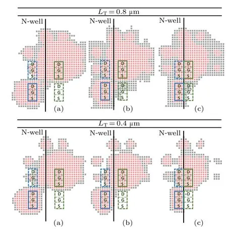
Fig. 11. For 33.2-MeV·cm2/mg ion irradiation, the SEU cross sections of SRAM cell with 0.8-μm, 0.4-μm LT and (a) 60-nm, (b) 40-nm, (c) 20 nm LM.

Fig.12. Comparison between cross sections with 0.8-μm and 0.4-μm LT.
It is found that narrowingLTcan exert much greater influence on NMOS cross section than on PMOS.This result supports our view. When 33.2-MeV·cm2/mg incident ion passes through SRAM cell,a large number of electron—hole pairs are generated. Under the action of well boundary electric field,electrons and holes are absorbed to the N-well and P-substrate respectively, thereby reducing the potential of N-well and increasing P-substrate potential. The reducing of potential difference at well boundary weakens the competitive effect of well boundary on charge collection at sensitive nodes. Improving the stability of taps to well potential can accelerate the electron and hole collection processes in the N-well and P-substrate respectively, restrain the weakening of boundary electric field and speed up its recovery. Therefore, improving the stability of taps can reduce the SEU cross section of NMOS.However,for the PMOS cross section,since the hole mobility is twice—thrice lower than that of electron,the hole collection process of PMOS is also prolonged (as shown in Fig.6,when incident ion is located at off-PMOS drain center,hole collection time is longer than electron collection time;when the incident point is far from the drain center, the difference in absorption time is further increased). In the whole process of PMOS hole collection, the ratio of the process of well boundary potential difference between reduction and recovery is much lower than in the process of NMOS, so the effect of shorteningLTon PMOS cross section is smaller.
4. Feasibility analysis
4.1. Tap distribution
For the SRAM hardening, compared with soft error induced by the SEU, the hard error caused by single event latchup(SEL)can induce device to be damaged,and thus leading to a greater danger.To prevent the SEL from occurring,the guard rings are adopted to mitigate parasitic silicon controlled rectifier(SCR)effect,which are placed between the group of PMOSs and the group of NMOSs as illustrated in Fig.13.

Fig. 13. (a) Solid and (b) intermittent guard rings in layout fragments of DICE SRAM blocks.[8]
The presence of guard rings limits the narrowing of NMOS and PMOS spacing. However, with the feature size scaling down and low power required in mobile applications,the supply voltage of the core circuit is usually below 1 V,which means that the latchup problem will not occur in the core circuits.[34]In addition to preventing the SEL,the guard rings, which act as taps, also inhibit the charge sharing, thus reducing the SEU cross section in DICE.[8]Therefore, for a combination of transistor location adjustment and DICE design, the guard ring cannot simply be removed, although the latchup problem is no longer a concern for the advanced Fin-FET technology.
Placing guard rings on the outside of NMOS and PMOS groups seems to be a good method, which can not only meet the requirements for narrowing the distance between NMOS and PMOS, but also inhibit the charge sharing. Besides, as mentioned in Subsection 3.3,the guard rings can also improve the stability of well potential, increasing the inhibiting effect of well boundary on SEU cross section in high LET ion irradiation.
4.2. Semiconductor processes
In our simulation, the distances between transistors and well boundary are set to be 60 nm, 40 nm, and 20 nm (LM).The 20-nm datum is cited from the report[35]issued by Intel, which demonstrates that the minimum transistor fin pitch is 42 nm. It is worth nothing that the minimum fin pitch is generally achieved between the transistors of the same type,like NMOS. Owing to the presence of well boundary between NMOS and PMOS,the minimumLMshould be slightly greater than half the minimum fin pitch. The simulation is intended to present the variation trend of SEU cross section withLM, where the 20-nmLMjust represents an extreme case. In the actual chip design process, theLMshould be minimized while meeting the design rule check(DRC)rules to reduce the SEU sensitivity of SRAM cells.
4.3. Scaling down of feature size
The device profile in Ref.[18]shows that the distance of 32-nm planar device and the distance of 22-nm FinFET device between NMOS and well boundary both decrease from 90 nm to 40 nm roughly. Meanwhile,the report[35]showed the metal pitch of logic area decreases by 30% (from 22 nm to 14 nm in feature sizes), where the metal pitch is linearly related to the distance between NMOS and well boundary. Furthermore,this trend will continue with scaling down(see in Fig.14).

Fig. 14. (a) Logic area scaling metric[35] and (b) metal interconnect pitch scaling.[34]
As mentioned in Subsubsection 3.2.1, there is a nonuniform potential distribution at the well boundary, and the electric field is stronger as it is closer to the boundary.With the increase of chip integration, the allowable minimum distance between MOSFET and the well boundary decreases. Therefore,it can be inferred that the influence of the well boundary electric field on charge collection of sensitive nodes is greater,and the inhibiting effect of reducing the spacing on cross section is stronger.
5. Conclusions
Reducing the spacing between well boundary and transistor can inhibit the charge collection at sensitive nodes of NMOS and PMOS, increase the restoring current of transistors and inhibit the bipolar effect of off-PMOS,which reduces the SEU cross section significantly. The TCAD simulations demonstrate that for the P-hit under the 33.2-MeV·cm2/mg ion irradiation, the cross section can be reduced by 55.2%, when the distance between MOSFET and boundary decreases from 60 nm to 20 nm. Unlike the DICE design, in the presence of enough taps to ensure the stability of well electrostatic potential,the inhibiting effect by the MOSFET location adjustment is more effective for cross section under the high LET ion irradiations. In consideration of the fact that for the core circuits of advanced FinFET devices the SEL will not occur and DICE designs are difficult to prevent SEU,the location optimization of the NMOS spacing and the PMOS spacing are useful for the SEU mitigation and can be used as a complement to DICE design.
Acknowledgement
Project supported by the National Natural Science Foundation of China (Grant Nos. 12035019, 11690041, and 62004221).
猜你喜欢
Chinese Physics B(2022年11期)2022-11-21
Chinese Physics B(2022年10期)2022-10-26
Chinese Physics B(2022年9期)2022-09-24
矿产勘查(2020年11期)2020-12-25
中国工人(2018年7期)2018-07-17
故事会(2018年11期)2018-06-08
美与时代·美术学刊(2018年10期)2018-01-25
小小说月刊·下半月(2017年7期)2017-07-25
民间故事选刊·下(2017年6期)2017-06-14
城市地理(2015年3期)2015-05-16

- Chinese Physics B的其它文章
- A nonlocal Boussinesq equation: Multiple-soliton solutions and symmetry analysis
- Correlation and trust mechanism-based rumor propagation model in complex social networks
- Gauss quadrature based finite temperature Lanczos method
- Experimental realization of quantum controlled teleportation of arbitrary two-qubit state via a five-qubit entangled state
- Self-error-rejecting multipartite entanglement purification for electron systems assisted by quantum-dot spins in optical microcavities
- Pseudospin symmetric solutions of the Dirac equation with the modified Rosen–Morse potential using Nikiforov–Uvarov method and supersymmetric quantum mechanics approach