
Gamma induced changes in Makrofol/CdSe nanocomposite films
2022-09-24 08:03AliAlhazimeMEBarakatRadiyahBaharethMahrousSaadAldawoodAbdElAalandNouh
Chinese Physics B 2022年9期
Ali A.Alhazime M.ME.Barakat Radiyah A.Bahareth E.M.MahrousSaad Aldawood S.Abd El Aal and S.A.Nouh
1Physics Department,Faculty of Science,Taibah University,Medina,Saudi Arabia
2Department of Physics,Faculty of Science,Taibah University,Yanbu,Saudi Arabia
3Department of Physics,Faculty of Science,Alexandria University,Alexandria,Egypt
4Physics Department,College of Science,Jeddah University,Jeddah,Saudi Arabia
5Department of Physics and Astronomy,College of Science,P.O.BOX 2455,King Saud University,Saudi Arabia
6Center of Radiation Research and Technology,Egyptian Atomic Authority,Nasr City,Cairo,Egypt
7Qassim University,P.B.6644,Buraidah 51452,Qassim,Saudi Arabia
8Physics Department,Faculty of Science,Ain Shams University,Cairo,Egypt
Keywords: gamma,nanocomposite,x-ray diffraction,UV spectra,color changes
1. Introduction
Today, polymeric nanocomposites (NCPs) containing polycarbonate (PC) have achieved huge awareness owed to their distinctive size that influences their behavior.[1]Numerous investigations have been carried out to design nano-sized materials of superior performance in different applications.[2,3]This has created a new era in reducing the price and enhancing the value of the next generation of developed applications.[4]Additionally, polymeric materials have achieved major awareness in practical applications due to their significant intrinsic character.[5]The limited absorbance bands and degradation of polymers have led to their use in optoelectronic devices.[2]The implementation of nanoparticles (NPs)treats any defect in polymeric matter by modifying their size and thus their usual reliability.[6]PC is a transparent polymer that has a suitably low density;thus it may be applied in many industrial tools like optical fibers and microelectronic apparatus. Nevertheless, enhancing the optical trend of PC is required to match novel industrial applications. Moreover,PC is a talented host material for many NPs. The impedance of NPs changes the character of PC without changing its toughness and transparency. The PC has unique characteristics allowing it to be a reasonable candidate in industrial requirements.[7,8]Additionally,minute NPs allow the investigation of appropriate surface properties due to their huge surface to bulk ratio.CdSe is an extensively used tunable and direct-bandgap (Eg)substance;itsEgis 1.74 eV estimated at 300 K.The huge Bohr exciton radius causes quantum confinement in CdSe. This makes those NPs significant, as they may be applied in optoelectronic applications.[9]
Additionally,γirradiation creates free radicals throughout degradation, and forms novel covalent bonds via crosslinks. Thus the polymer’s macro-molecular and morphological structures are affected without modifying their configuration.[10]Consequently, lattice defects are generated that create sensitive type, modifying the NCP character.[5]These modifications are dependent on the structure of the matter.[11]
Furthermore, the color changes in the NCP samples due toγradiation are necessary parameters that evaluate the optical modification in the NCP substance. This is an essential factor in industrial applications.[12]Several authors have performed studies on the use of polymeric NCP films in dosimeter applications through studying their modification in optical properties.[13-16]They accredited the modification in color in irradiated PC to the rearranged isopropylidene radicals,strong conjugated bonds, and production of active free radicals and benzophenones.[17]
In the current study,CdSe NPs have been selected owing to their direct intrinsicEgthat allows them to be an essential substance in several applications.[18]Consequently, the CdSe NPs can be embedded inside the PC matrix,enhancing its optical properties.[19]Additionally,PC was elected as a host matter for these NPs because PC assists in different applications showing excellent chemical resistance.[7]The PC-CdSe NCP is treated via radiation processing as it is a convenient technique that induces reasonable alterations of polymer NCPs. In particularly, it is an essential route to attaining some favorable improvements for several applications in a wide range of industrial fields. Our current study aims to prepare NCP of CdSe@PC to illustrate the possibility of enhancing its performance in numerous industrial applications.
2. Experimental details
2.1. Preparation of CdSe NPs
Nanomaterials attained by a thermolysis technique are extensively used in several prominent fields.[20-22]This is realized from easy manufacture of NPs by a thermolysis procedure producing properties including a large active surface area,enhanced porosity, size selectivity, exact surface composition,high photocatalytic activity and high adsorption capacity. We prepared CdSe NPs by applying the thermolysis procedure described in Ref.[23]. CdO(0.45 g)and stearic acid(9 g)were merged in a flask (three-necked) and heated at 150°C in the presence of N2gas flow until completely dissolved. Then hexadecylamine(12 g)and trioctylphosphine oxide(TOPO)(8 g)were added with strong rousing(30 min at 120°C).After that,we dissolved Se powder (0.78 g) in TOPO (9 ml) and then speedily added it. A gradual increase in temperature(120°C-220°C) formed monodisperse CdSe. Lastly, CdSe was precipitated with methanol and unglued applying a centrifuge.Then we washed out the resultant substance using methanol and chloroform many times.
2.2. Preparation of the PC–CdSe NCP
Several methodologies can be applied to prepare polymer NCPs. These procedures can be melt intercalation, template synthesis,exfoliation adsorption andin situpolymerization intercalation.[24,25]Melt intercalation is the distinguishing usual one owing to being environmentally agreeable. It is also well matched with industrialized means.[24,25]Theex situcasting procedure used for preparing NCP matter delivers nanosize matter that is a suitable candidate for device applications in various fields.[2,3]
Makrofol DE 7-2 polybisphenol-A-carbonate (PC) of chemical composition C16H14O3was manufactured by Bayer A.G.,Leverkusen(Germany). Chloroform was used as a solvent to PC with extensive rousing for 120 min at room temperature(RT)until obtaining full dissolution. Then,we dissolved 2 g of PC in 30 mL chloroform. The product solution was added to the pre-prepared NPs(0.5 wt%)with extensive rousing to obtain the NCP by means of the mathematical equation
wherewpandwfare the weights of the PC and CdSe NPs,respectively. We then cast the mixture into Petri dishes, and dried it for two days at 60°C to wholly get rid of impurities.Finally,NCP films of nearly 0.3 mm thickness were formed.
To recognize the mechanism of CdSe NP formation and how the metallic ions, Se2-and Cd2+, interacted, it was predictable that full mixing of the raw materials in the prepared solution would promote the combination of the metallic ions with the carbonyl group present in polymeric chains. Subsequently, drying removed water from the mixture, solidifying the metallic cations in the polymer cavity.[26]
2.3. Irradiation tool
The PC-CdSe NCP films have been irradiated withγdosage 20 kGy-250 kGy by means of60Co equipment(Canada Ltd.) with series of 1.173 MeV-1.332 MeV at
2.4 Gy/min(A,E.A.,Egypt).
2.4. Instrumentation
X-ray diffraction (XRD) was conducted using a diffractometer (model: X’Pert-Pro MPD; Philips, Eindhoven, The Netherlands)with a goniometer via Cu-Kαradiation. To correct the instrumental widening we applied standard LaB6. The composition and micro-composition of the crystal were polished by means of a Rietveld outline procedure,[27]applying the program MAUD.
The morphology of the NPs were explored by transmission electron microscopy (TEM) on a JEOL TEM (model:JSM2010;JEOL Ltd.,Tokyo,Japan).
The absorbance was measured (200 nm-800 nm) by applying a Shimadzu UV spectrophotometer (type 3101 PC,Berkshire,UK).The CIE process was used for signifying the colored samples. The CIELAB color difference parameters were estimated using the mathematics previously described by us.[28]
3. Results and discussion
3.1. Structural investigation of γ irradiated PC–CdSe NCP
Rietveld enhancement of the XRD outline of CdSe applying the MAUD program is displayed in Fig.1(a).The prepared CdSe adopts a cubic zinc merger structure of 6.057 ˚A lattice parameter and a typical grain size of 2 mm. The TEM image of the CdSe NPs is displayed in Fig. 1(b). The profile of the CdSe dotted outline approved an enhanced size of nearly 2 nm,confirming the quantum dot balance of CdSe.

Fig. 1. (a) XRD outlines fitting resultant from Rietveld analysis of CdSe quantum dots,(b)TEM image of CdSe NPs.
XRD was performed to investigate the modifications induced in the mass fraction of the amorphous phase due toγirradiation. The XRD patterns of the irradiated PC-CdSe and pristine films in the 2θseries 10°-30°are shown in Fig. 2.The patterns of the films are characterized by the presence of a distinctive wide amorphous peak expanding in the 2θrange 13°-25°denoting that the NCP film is a partially crystalline with major amorphous regions. Although the concentration of CdSe NPs in the PC-CdSe NCP was 0.5 w%, no diffraction pattern is obtained for CdSe NPs and thus the wide peak should belong to PC. Heibaet al.[29]obtained the same trend of CdSe with PMMA polymer. They found no difference between pure PMMA and PMMA loaded with CdSe NPs,and hence no diffraction pattern obtained for CdSe NPs.They attributed this trend to the homogeny of distribution of CdSe NPs throughout the PMMA. They also investigated that if CdSe was clustered,a diffraction pattern would be obtained even if its amount was small. The investigation that the obtained wide peak should belong to PC could be confirmed by comparison with our recent study on pure Makrofol polymer.[30]The patterns of the pristine Makrofol film indicated the presence of the same wide peak expanding in the same 2θrange 13°-25°.
The bands of the samples were fitted using a Lorentz function. Therefore,the area of the wide diffraction peak(integral intensity,I)was calculated and is represented in Fig.3.The integral intensity increased up to a maximum value around 50 kGy due to initial chain scissions. This means that theγradiation with 50 kGy dosage causes the degradation of carbonate and isopropyl groups in the PC chains,and then decomposition of aromatic rings occurs.[28]This allows the reduction of both the intermolecular stress in the disordered region and the number of entanglements per molecule, hence enhancing the chain mobility allowing molecules to be reordered.[13]The integral intensity decreased due to the destruction of the ordered structure via crosslinks when irradiating above 50 kGy and up to 250 kGy. This indicates that theγradiation converts the regularly arranged lamellas into non-arranged ones through crosslinks.
Since the width of the halo at half maximal intensity(ΔW)is inversely proportional to the crystallite size (L), the values of ΔWwere estimated by means of the Scherrer formula

whereλis the wavelength of the x-rays. The dependence of ΔWon theγdosage is displayed in Fig. 3. ΔWshows similar values within experimental error,meaning that the width of the lamella is not affected by theγdosages.

Fig.2. XRD outlines of the pristine and irradiated PC-CdSe NCP films.

Fig.3. Variation of I and ΔW with the γ dosage.
3.2. Optical investigation of γ irradiated PC–CdSe NCP
3.2.1. Absorption study
The absorbance spectra of the irradiated and pristine PCCdSe films were demonstrated to estimate the alternations in the bandgap configuration owing toγradiation (Fig. 4). The alternation of absorbance withγdosage is attributable to the persuaded modification in the energy band owing to irradiation together with the Rayleigh scattering from the implanted CdSe NPs.[31]A higher absorption band appeared at close 280 nm-310 nm that decreased with increasing wavelength up to 800 nm. The reduction of absorbance with increasing wavelength is attributable to the n-π∗transition C=O (carbonyl group)andπ∗-π∗(phenyl group).[32]The formation of color centers (310 nm-320 nm) can also be a reason.[33]At the wavelength 290 nm, the photochemical reactions formed in the PC matrix activated the singlet or triplet state of the macromolecules.[30]At 320 nm-400 nm, the C-H bond was cracked owing toγirradiation. At 290 nm-315 nm,the bonds matching to energy smaller than 4.5 eV and 6.2 eV were destroyed owing to theγdosages.[34]Moreover,the absorbance rose on raising the dosage up to 250 kGy owing to the growing conjugated bonds[35]. The tiny size of the NPs gives them a much larger surface area to volume ratio which is an important feature for reactivity,that is,the rate at which the chemical reaction will proceed,because more surfaces are vacant to react and assist chemical processes.[36]Accordingly,the atomic volume full of NPs reduces,hence its density and absorbance increase.[37]In other words, the increase in absorbance with increasingγdosage denotes the absorption of the incident photon energy by the NCP intermediate atoms.In addition,the energy transferred by the incidentγradiation may create a new chemical arrangement that leads to an increase in absorbance.Moreover, the existence of extra negative charges forms new interior bonds in the NCP due to crosslinks.
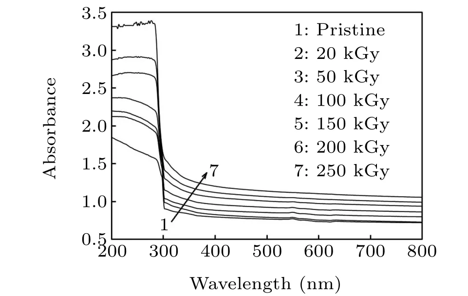
Fig.4. Absorbance spectra of the irradiated and pristine NCP films.
The extinction coefficient (k) is an important parameter that provides information about the spreading and incorporation resources of the penetrated area. The compound part of the refractive index can be calculated from The absorbance coefficient(α)stands for the quantity of photons absorbed by matter, and hence it is used to illustrate the variations in band construction.

3.2.2. Bandgap study
The numerical values of the bandgap (Eg) have been estimated by means of Tauc’s principle for direct transition,which provides information concerning the transitions inEgconfiguration,[38]

whereBis a constant,hνis the energy of the incident photons andnis an index; its value signifies the trend of electronic transition.nequals 1/2 or 3/2 for direct transitions, whilenequals 2 or 3 for allowed or forbidden indirect transitions.[39]Egis valued by scheming(αhν)1/nversushν;the former induces the linear portion of the curvature to meet thehνaxis(Figs.5-7).

Fig.5. Plot of(αhν)2 versus hν for the irradiated and pristine NCP films.

Fig.6. Plot of(αhν)0.5 versus hν for the irradiated and pristine NCP films.
The bandgap of the pristine PC-CdSe NCP is 4.15 eV(n=0.5),which is rather less than the values that were previously published for pristine PC film(4.44 eV).[40]This reduction is attributable to the presence of NPs that support the deficiencies to change the inner construction ofEg.[40]The dependence of the directEgof the PC-CdSe films on theγdosage is shown in Fig.8(using the data represented in Fig.5). The bandgap decreased on growing theγdosage to 250 kGy. This decrease inEgis due to crosslinking. Therefore, the amorphous phase of the PC-CdSe NCP is augmented through persuading defects and as a result forward localized states are presented in theEgsystem, which causes electronic transitions with less energy. The consequential outcome ofγon the NCP films is the production of chemically active free radicals that cause crosslinking. On raising theγdosage, the creation rate of free radicals rises, increasing the unsaturated and conjugated bonds and thus decreasingEg.[35]

Fig.7. Plot of(αhν)2/3 versus hν for the irradiated and pristine NCP films.

Fig.8. Variation of Eg and Eu with γ dosage.
Figures 5-7 obtained from Tauc’s model together with the optical dielectric loss function represented in Fig.9 were considered to deduceEgand the type of electronic transition.This is because the optical dielectric constant is enormously influenced by the band structure of the material. In addition, the investigation of dielectric loss by applying UV spectra is considerably helpful in assuming the whole band construction of matter.[41]The imaginary portion ofε''is useful for investigating the electronic transition among occupied and unoccupied states.[39]Theε''values were valued applying the formula

Theε''spectra obtained for the pristine and irradiated PCCdSe NCP samples is shown in Fig.9.TheEgvalues obtained fromε''are significantly near to those obtained from Tauc’s model as seen in Table 1. Therefore, the type of electronic transition is the allowed direct transition.[41]

Table 1. Optical bandgap (from Tauc’s model and ε'' versus hν) for the non-irradiated and irradiated PC-CdSe NCP films.

Fig.9. Plot of ε'' versus hν for the irradiated and pristine NCP films.
3.2.3. Urbach energy study
Urbach energyEuinvestigates the building of materials through the judgment of the deficiency altitude in the forbiddenEg. TheEuvalues were computed using the formula[42]

whereEuexpresses the degree of disorder andαois a constant.[43]By scheming lnαverseshνwe can deduceEufrom the inverse of the slope of the resultant straight line.TheEuvalues increased from 0.16 eV to 0.28 eV on increasing the dosage up to 250 kGy (Fig. 8). The increase inEuis attributable to the rise of the disorder character via crosslinks.[44]
3.2.4. Refractive index study

The refractive indexn,of the PC-CdSe NCP films is estimated from the formula[45]Figure 10 shows the change in refractive index withγdosage.The refractive index rose on increasing the dosage up to 250 kGy. This trend is in agreement with that ofEgmeaning the authority of crosslinks. The chain scissions create lively free radicals that permit the creation of covalent bonds via crosslinks. This explanation is in good agreement with that obtained previously.[46,47]
Mostly,the dielectric properties provide information concerning the optical characteristics of materials.[48]The dielectric constant varies withhν,signifying that certain interactions between photons and electrons occur in that energy range.
The dielectric constant (ε') is calculated from the equation[49]

Theε'values are plotted in Fig. 11 against wavelength.ε'rises with increasing dosage up to 250 kGy. This denotes the growth of the density of states within the forbidden gap of the PC-CdSe NCP due toγirradiation.[50]

Fig.10. Variation of n with γ dosage.

Fig.11. Plot of ε' versus hν for the irradiated and pristine NCP films.
3.3. Color alternations study
The transmittance spectrum of the irradiated and pristine PC-CdSe NCP films(370 nm-780 nm)is displayed in Fig.12.The real red,green and blue lights are represented by the setsX,Y, andZ, which are known as tristimulus values.[51]The chromaticity coordinates and tristimulus values were valued using the transmittance records 370 nm-780 nm (Table 2).The tristimulus values reduced with increasing dosage up to 250 kGy. The values ofxandyimproved on increasing the dosage up to 250 kGy. Thezcoordinate showed an inverted trend.
The CIELAB color intercepta∗compares the red (+a∗)and green (-a∗), while the interceptb∗compares the yellow(+b∗) and blue (-b∗).L∗expresses the lightness. A faultless white has anL∗of 100, and a faultless black has anL∗of 0. The accuracy in estimatingL∗is±0.05 and±0.01 fora∗andb∗respectively. The variation of color intercepts withγdosage is represented in Fig. 13. The color interceptsa∗andb∗exhibited negative values that augmented with increasing dosage up 250 kGy. This specifies that the green and blue color components tend to turn to red and yellow,respectively(Fig. 13(a)). This is related to the growth in darkness in the PC-CdSe(-L∗)(Fig.13(b)).

Table 2. Tristimulus values(X,Y,and Z)and chromaticity coordinates(x,y,and z)of the PC-CdSe films as a function of γ dosage.
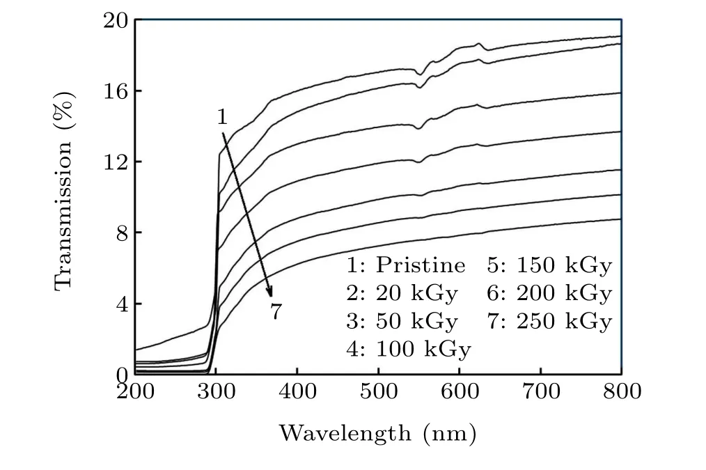
Fig.12. Transmission spectra for the irradiated and pristine NCP films.

Fig.13. Variation of color intercepts and color intensity with γ dosage.
The color intensity(ΔE),which represents the difference in color between the pristine and irradiated films,is calculated using the formula used before.[29]Its variation is displayed in Fig. 13(b) againstγdosage. ΔEimproved on increasing theγdosage up to 250 kGy. The values of ΔEattained a noteworthy color alteration, which is a satisfactory feature in saleable reproduction on printing presses,as ΔEis bigger than 5.[52,53]This shows that the PC-CdSe NCP has a tendency to color transformation byγirradiation. The color fluctuations are produced by the hot free radicals that are shaped by chain scissions. Moreover,the hot free radicals have electrons with unpaired spin origin color discrepancies.[29]
4. Conclusion
Theγirradiation of PC-CdSe films leads to the dominance of crosslinks, which modifies their structural and optical properties. Increasing theγdosages from 50 kGy to 250 kGy leads to an increase in the mass fraction of the amorphous phase, reflected in a reduction in the values of the optical bandgap, linked with an increase in the refractive index and optical dielectric constant. These optical alternations may optimize PC-CdSe NCP films for optoelectronic applications.Furthermore, the PC-CdSe NCP films can be an adequate match in marketable imitation in printing presses.
Acknowledgment
Researchers Supporting Project Number (RSP-2021/328),King Saud University,Riyadh,Saudi Arabia.
- Chinese Physics B的其它文章
- Characterizing entanglement in non-Hermitian chaotic systems via out-of-time ordered correlators
- Steering quantum nonlocalities of quantum dot system suffering from decoherence
- Probabilistic quantum teleportation of shared quantum secret
- Spin–orbit coupling adjusting topological superfluid of mass-imbalanced Fermi gas
- Improvement of a continuous-variable measurement-device-independent quantum key distribution system via quantum scissors
- An overview of quantum error mitigation formulas