
Migration of weakly bonded oxygen atoms in a-IGZO thin films and the positive shift of threshold voltage in TFTs
2022-09-24 08:00ChenWang王琛WenmoLu路文墨FengnanLi李奉南QiaomeiLuo罗巧梅andFeiMa马飞
Chinese Physics B 2022年9期
关键词:马飞
Chen Wang(王琛), Wenmo Lu(路文墨), Fengnan Li(李奉南), Qiaomei Luo(罗巧梅), and Fei Ma(马飞)
State Key Laboratory for Mechanical Behavior of Materials,Xi’an Jiaotong University,Xi’an 710049,China
Keywords: a-IGZO thin films,weakly bonded O atoms,threshold voltage shift
1. Introduction
The development of high-resolution and flexible display technology depends heavily on the channel materials of thinfilm transistors (TFTs). Amorphous indium-gallium-zinc oxide(a-IGZO)has attracted much attention due to its high mobility and potential application in flexible devices.[1-3]However,the shift of threshold voltage(Vth)of a-IGZO TFTs under positive gate bias is still a critical issue. The positiveVthshift in TFTs has been ascribed to the negative charges accumulated at the a-IGZO/insulator interface and the screened gate electric field.[4-7]The negative charges could come from electrons trapped in the gate dielectrics[8]or acceptor-like states.Electron trapping in gate dielectrics commonly occurs in TFTs with high-permittivity gate dielectrics,so it is not widespread.Nomuraet al.attributed theVthshift to shallow trap states.[9]Chowdhuryet al.carried out a time-temperature dependence experiment,and attributed theVthshift to defects corresponding to the fitted activation energy,but the fitting accuracy was limited by the narrow temperature range (27°C-90°C).[10]Umet al.observed a hump in the subthreshold region of the transfer curves under positive gate bias, and ascribed it to the acceptor-like states near the a-IGZO/insulator interface.[11]Apparently, the mechanism for theVthshift is still controversial. Furthermore,those mechanisms cannot be adopted to explain the effect of ambient O2on theVthshift. To understand the ambient effect,Zhouet al.proposed a model of chemically adsorbed O2.[12]Chenet al.found that the activation energy of O2adsorption could be lowered by gate bias,resulting in aVthshift in an O2atmosphere.[13]Xuet al.illustrated that the ambient O2could compensate for the oxygen vacancies and improve the subthreshold performance.[14]In other words, a contradiction still exists regarding the effect of ambient O2,and it is still not understood why and how the adsorption of O2at the back channel can induce acceptor-like states at the a-IGZO/insulator interface.
In this work, a-IGZO thin films are prepared by pulsed laser deposition (PLD) and are fabricated into TFT devices.The morphology, phase structure, and chemical states of the a-IGZO thin films are characterized,and the influences of the deposition O2pressure, vacuum annealing temperature, ambient O2,and film thickness on the electrical properties of the a-IGZO TFTs are investigated;in particular,theVthshift under positive gate bias is discussed. Furthermore,in-situx-ray photoelectron spectroscopy(XPS),a temperature variation experiment and anin-situvacuum annealing experiment were carried out to understand the mechanism responsible for theVthshift of the a-IGZO TFTs. It was found that theVthshift could be attributed to the deep acceptor-like states induced by the accumulation of weakly bonded O atoms at the a-IGZO/SiO2interface.
2. Experiment
2.1. Preparation and characterization of a-IGZO thin films
The a-IGZO thin films are prepared by the pulsed laser deposition (PLD) technique using a KrF excimer laser(248 nm,~10 J·cm-2per pulse). The target is a homemade crystalline IGZO ceramic (In:Ga:Zn:O=2:2:1:7 mol%)sintered at 1400°C.The surface morphology of the a-IGZO thin films is observed using a scanning electron microscope(SEM)and the phase structure is characterized by xray diffraction(XRD,λ=1.5406 ˚A).An interconnected XPS and PLD system in a vacuum chamber is used forin-situcharacterization of the elemental contents and chemical states to avoid contaminants and adsorbates. The excitation source for the XPS is AlKαwith an energy of 1486.6 eV. The sample is heated in an analysis chamber, which has a better vacuum than 1.0×10⁻⁵Pa. The XPS spectra of O 1s in the interior and on the surface of the thin film are measured by changing the photoelectron collection angle from 90°to 30°.
2.2. Fabrication of TFTs and details of the electrical measurement
The a-IGZO TFTs with a top contact and a bottom gate (p+-Si substrate) are fabricated. The insulator consists of 280 nm of thermally oxidized SiO2, and 100 nm Mo source/drain electrodes are deposited by radio frequency(RF)magnetron sputtering.In-situelectrical measurements of the TFTs are carried out using a homemade probe station in vacuum. The probe station is pumped by a molecular pump unit.Pure O2gas can be introduced into the station. Alumina ceramic heating plates and K-type thermal sensors are attached to the samples and the temperature is regulated by an Eurotherm 3504 controller. In this setup, four samples can be measured at the same time by a combination of a Keithley 2700 matrix switcher and a 2612b source meter. The transfer curves can be measured after thermal annealing in a vacuum better than 10-4Pa. The temperature variation measurements are implemented in a He exchange cryostat.The sample is cooled by the circulation of helium around a closed circuit driven by a dry pump. The helium gas is cooled by the cryo cooler to the 40 K and 4 K stages and then cooled further via expansion from the needle valve. A heat exchanger is used to adjust the temperature of the helium gas,and thus the sample temperature is controlled in the range of 20 K-300 K.All the electric measurements are done in the dark.[15,16]
Transfer curves are measured by sweepingVgfrom-60 V to 60 V in steps of 0.5 V,withVdkept at 2 V.To evaluate theVthshift, a constant gate voltage (Vg) of 60 V and a drain voltage(Vd)of 2 V are biased for 400 s after each transfer curve measurement. For the recovery process,the a-IGZO TFTs are electrically disconnected for 400 s and theVgsweeping is stopped whenIdis larger than 5 nA,taking the turn-on voltage(Von)shift to represent theVthshift. TheVthis calculated through the transfer curve
in whichLandWare the channel length and width, respectively,Coxis the unit area capacitance of the insulator dielectrics,andVdis the drain voltage.Vthis determined by fitting the linear region of theId-Vgcurves. The field effect mobility(µ)is obtained by fitting the linear region of the transfer curves
2.3. Gr¨unewald method
The Gr¨unewald method is adopted to extract the density of states(DOS)of a-IGZO from the transfer curves. The starting point for this method is the 1D Poisson equation

The flat band voltage is considered to be approximately equal toVonwhen the source-drain current is 5 nA. The extraction of the DOS is carried out in Matlab.
3. Results and discussion
3.1. Characterization of the a-IGZO thin films
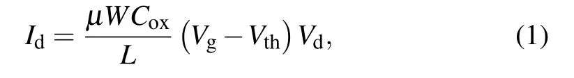
Figure 1 shows SEM images of the a-IGZO thin films.Evidently, the film surface is smooth if the deposition pressure is lower than 6 Pa, but clusters appear on the surface at a deposition pressure of 10 Pa, and the thin films become rough. Therefore,deposition pressures in the range of 2.0 Pa-4.5 Pa can avoid the influence of surface roughness. Figure 2 shows XRD patterns of a-IGZO thin films deposited at oxygen pressures of 1 Pa-10 Pa and annealed at 373 K-873 K.As displayed in Fig. 2(a), no sharp peak can be identified in the patterns, confirming the deposition-pressure-independent amorphous characteristic of a-IGZO. Furthermore, as shown in Fig. 2(b), the amorphous structure can be thermally stable at up to 673 K. Therefore, the effects of phase structure and transition on the electric performance can also be excluded.
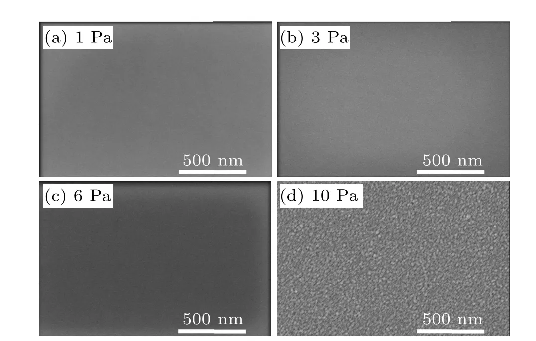
Fig.1.SEM images of a-IGZO thin films deposited at different O2 pressures:(a)1 Pa,(b)3 Pa,(c)6 Pa,and(d)10 Pa.
To further understand the influence of deposition pressure and vacuum annealing on the a-IGZO films,in-situXPS is carried out, and the results are shown in Fig. 3. The O 1s spectrum is deconvoluted by the Voight function into two peaks at 531.0 eV (the OIpeak) and~532.5 (±0.1) eV (the OIIpeak) in Fig. 3(a). A peak (peaks) corresponding to surface impurities is(are)not in evidence;in other words,in-situcharacterization can avoid the influences of surface impurities on the O1s spectrum. The OIpeak originates from the lattice oxygen atoms, which are tightly bonded with surrounding In atoms in the form of In-O6.[17]As shown in Fig.3(b), the O content of IGZO thin films deposited at oxygen pressures of 1 Pa-5 Pa oxygen pressure is greater than 58.3%(corresponding to the stoichiometric ratio in In2Ga2ZnO7),indicating the presence of excess O atoms in a-IGZO thin films. The bond length between the weakly bonded O atoms and the surrounding In atoms is considerably larger than the normal In-O bond(0.211 nm), with less charge transfer from In to O atoms and thus a higher binding energy of O 1s.[18]Therefore, the OIIpeak originates from the weakly bonded O atoms rather than

Fig.2. (a)XRD patterns of a-IGZO thin films deposited at different O2 pressures,namely,1 Pa,3 Pa,6 Pa,and 10 Pa. (b)XRD patterns of a-IGZO films deposited at a pressure of 3 Pa of O2 and annealed at 373 K,473 K,673 K,and 873 K in vacuum for 12 hours.

Fig.3. In situ XPS analysis of a-IGZO films. (a)O 1s spectrum of a-IGZO deposited at a pressure of 3.0 Pa of O2. (b) The O content and (c) the area ratio of OII/OI in a-IGZO thin films deposited at different O2 pressures. (d)The area ratio of OII/OI in a-IGZO thin films deposited at a pressure of 5 Pa of O2 and annealed at different temperatures. (e)The area ratio of OII/OI in a-IGZO thin films deposited at a pressure of 5 Pa of O2,collected at 90° and 30°,and then annealed at 400 °C.
oxygen vacancies. The content of weakly bonded O atoms increases with the deposition pressure(Fig.3(c)),but decreases with increasing annealing temperature in vacuum (Fig. 3(d)).
The content of weakly bonded O atoms both in the interior and on the surface increases once the annealed a-IGZO thin films are exposed to 105Pa ambient O2for 12 hours (Fig. 3(e)).Therefore,the increment of weakly bonded O atoms is caused by the migration of ambient O2into the a-IGZO thin films,but not by the adsorption of O2.
3.2. The influence of deposition pressure on the Vth shift
Figure 4(a) schematically displays the cross-section of the a-IGZO TFTs. Figure 4(b) shows the output curves of a-IGZO TFTs deposited at an oxygen pressure of 3.0 Pa,and the TFTs are in the linear region at aVdof 2 V. Figure 5 shows the transfer curves of a-IGZO TFTs under positive gate bias.TheVthshift is evidenced in all the a-IGZO TFTs, and increases remarkably with deposition pressure. As mentioned above, the number of weakly bonded O atoms also increases with the deposition pressure. On the whole,theVthshift might be ascribed to the acceptor-like states induced by the weakly bonded O atoms.[19]In essence,theVthshift occurs if electrons are trapped in acceptor-like states.
Fig.4. (a)Schematic cross-section of a-IGZO TFTs. (b)Output curves of an a-IGZO TFT deposited at a pressure of 3 Pa of O2.
3.3. Temperature variation experiment
A temperature variation experiment is carried out to study the thermally activated process of theVthshift. As shown in Fig. 6(a), the TFTs exhibit normal transfer curves at 20 K-300 K,both the mobility andVonchange significantly for temperatures of 200 K or less,but are almost temperature independent at 200 K-300 K (Fig. 6(b)). A series of transfer curves are measured under positive gate bias and at different temperatures.The difference between theVthvalues with and without bias(ΔVth)is used to quantitatively describe theVthshift. As displayed in Figs. 6(c) and 6(d), theVthshift is thermally activated, and the temperature-dependentVthshift is a good fit for an activation model,i.e.,ΔVth=Aexp(-Ea/kT). The activation energies of theVthshift and the recovery process are fitted to 144 meV and 195 meV,which are close to the activation energy of oxygen diffusion in a-IGZO (~100 meV).[20]Accordingly, it is proved that theVthshift of a-IGZO TFTs is induced by the accumulation of weakly bonded O atoms at the a-IGZO/SiO2interface under positive gate bias. It should be noted that the migration of weakly bonded O atoms is not significant at 200 K or below,and thus theVthshift at low temperature is mainly controlled by the electrons trapped in the pre-existing acceptor-like states,which have quite small thermal activation energies.
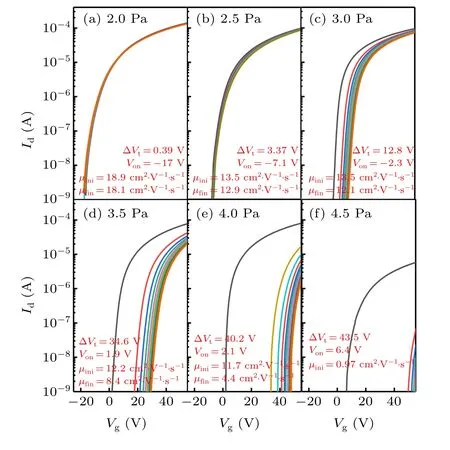
Fig.5.Transfer curves(Id-Vg)of a-IGZO TFTs with 50 nm a-IGZO thin films deposited at different O2 pressures and measured under positive gate bias.
3.4. The influences of ambient O2 on the Vth shift
Ambient O2could also induce theVthshift.[12-14,21]Insituvacuum annealing and measurement are implemented to study the influence of ambient O2on theVthshift by allowing O2at different pressures into the vacuum chamber afterin-situannealing. Figure 7 displays the transfer curves of a-IGZO TFTs annealed at 383 K-398 K in a better vacuum than 10-4Pa for 12 hours. A remarkableVthshift occurs in the TFTs annealed at 383 K,while deteriorated subthreshold performance is observed in the TFTs annealed at 393 K and 398 K because of the large number of oxygen vacancies induced by vacuum annealing at higher temperatures.Accordingly,388 K is the optimal vacuum annealing temperature. Figure 8 shows the transfer curves of TFTs with 10 nm IGZO films deposited at an oxygen pressure of 3.0 Pa and annealed at 388 K, then exposed to O2at a pressure of 10-4Pa-105Pa. Since the film thickness is smaller than the Debye length in the subthreshold region(~11 nm),the effect of adsorbed O2can be observed in the transfer curves.[12]After vacuum annealing, the mobility of the TFTs is remarkably improved from 13.5 cm2·V-1·s-1to 31.4 cm2·V-1·s-1. Compared with the deposited TFTs,the TFTs annealed in vacuum at a pressure of 10-4Pa do not exhibit theVthshift,indicating that the weakly bonded O atoms are eliminated,which is also confirmed by thein situXPS.As the ambient O2pressure increases,Vonmoves positively,even at low O2pressures, as a result of a depletion layer induced by O2adsorption.[22]However,a considerableVthshift occurs only at high ambient O2pressures,which cannot be explained by O2adsorption. Taking this into account, it is further confirmed that theVthshift of a-IGZO TFTs in ambient O2can be ascribed to the migration of weakly bonded O atoms from ambient O2into the a-IGZO thin films, as confirmed by thein-situXPS spectra.

Fig.6. Temperature dependence of transfer curves and the Vth shift. (a)Transfer curves at 20 K-300 K.(b)Field-effect mobility and turn-on voltage.(c)and(d)The Vth shift as a function of temperature in the bias and recovery processes in linear and logarithmic coordinates,respectively.
3.5. The migration of ambient O2 controlled by the a-IGZO thickness
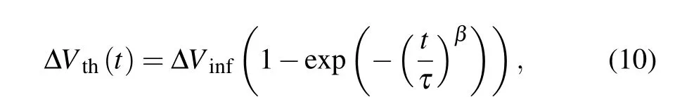
Given that theVthshift is caused by the migration of ambient O2,the thickness of the a-IGZO films might affect theVthshift substantially. Thus, theVthshift of TFTs with a-IGZO thicknesses of 12 nm-95 nm are fitted to a stretched exponential function[23]in which ΔVinfis theVthshift at infinite time,tis the time,τis the time constant,andβis the exponential factor.The fitted results are plotted in Fig.9;ΔVinfandτare used to quantitatively describe theVthshift. As the thickness of a-IGZO thin films is increased,ΔVinfdecreases andτincreases,suggesting a reducedVthshift, which can be ascribed to the suppressed migration of ambient O2in the thicker a-IGZO films. A critical thickness of 50 nm is enough to avoid the influence of ambient O2. Theβvalue of 0.4 is maintained for different thicknesses,which means that the migration of weakly bonded O atoms is dominated by a short-range force.[24]

Fig.7. Transfer curves(Id-Vg)of 10 nm a-IGZO TFTs annealed in vacuum at different temperatures: (a)383 K,(b)388 K,(c)393 K,and(d)398 K.
Fig. 8. Transfer curves (Id-Vg) of 10 nm a-IGZO TFTs biased at different ambient O2pressures and measured under positive gate bias.
3.6. Deep acceptor-like states generated by weakly bonded O atoms
The acceptor-like states in a-IGZO can be divided into two types, shallow states and deep states.[25]The DOS of shallow states is extracted from the transfer curves using the Gr¨unewald method,[26,27]and the results are plotted in Fig.10.For a-IGZO films annealed in vacuum,the ionized oxygen vacancies(V2+O)induce shallow acceptor-like states at~0.1 eV above the Fermi level,[28]as shown in Fig.10(a). Oxygen vacancies affect the electrical properties of a-IGZO TFTs significantly, and can result in a negativeVthshift.[14,28]However,the positiveVthshift cannot be ascribed to oxygen vacancies(VO). If the positiveVthshift is closely related to VO,and VO,as the shadow donors,could provide free carriers,the turn-on voltage should become more negative with a larger positiveVthshift at a higher oxygen vacancy concentration, which is in contradiction to the experimental results in this work. As shown in Figs.5 and 8,if the a-IGZO thin films are deposited at lower oxygen pressures or exposed at lower ambient oxygen pressures, more VOis involved, but the TFTs exhibit a more stableVthunder a positive gate bias. Therefore,the positiveVthshift is not directly related to oxygen vacancies. On the other hand, the carriers in TFTs are confined to a thin region(~1 nm)close to the dielectrics,and will be scattered by deep trapped electrons at the a-IGZO/SiO2interface. Therefore,the reduced mobility in Figs.5 and 8 corresponds to the deep trapped electrons at the a-IGZO/SiO2interface.[19,29]

Fig.9. The Vth shift of TFTs with different a-IGZO thicknesses tested in an O2 atmosphere;the values of Vth at infinity(ΔVinf),the time constant(τ),and the exponential factor (β) are extracted by fitting the stretched exponential equation.

Fig.10. Density of states(DOS)with respect to the Fermi level extracted by the Gr¨unewald method. (a)DOS of TFTs before bias at different ambient O2 pressures. (b)-(f) DOS of TFTs biased at 10-4 Pa, 60 Pa, 200 Pa, 104 Pa,and 105 Pa,respectively.
Figure 11 schematically shows a physical picture of the positiveVthshift in a-IGZO TFTs. As displayed in Figs.11(a)and 11(b), the weakly bonded O atoms in the a-IGZO thin films migrate towards the a-IGZO/SiO2interface under a positive gate bias and induce deep acceptor-like states at the interface. The electrons trapped in the deep acceptor-like states will screen the gate field, leading to a potential step and the positiveVthshift.However,the oxygen-vacancy-related mechanism(Figs.11(c)and 11(d))cannot be adopted to adequately interpret the screening effect on the gate electric field.
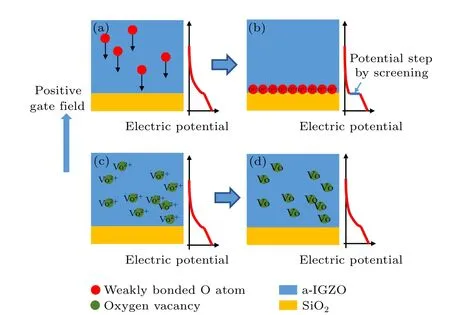
Fig.11. Schematic diagram of the positive Vth shift in a-IGZO TFTs. (a)and(b)A model of the weakly bonded O atom migration under the gate electric field. (c) and (d) A model of ionized oxygen vacancies capturing electrons under the gate electric field.
4. Conclusion
In this work,a-IGZO thin films are prepared by PLD,and a-IGZO TFTs are fabricated. The morphology, phase structure, and chemical states of the a-IGZO thin films are characterized.In-situXPS demonstrates that weakly bonded O atoms are induced in a-IGZO thin films at high deposition pressures, but can be eliminated by vacuum annealing. High deposition pressures lead to largeVthshifts, and the activation energy of theVthshift is fitted to 144 meV as part of the temperature variation experiment. Accordingly,theVthshift is caused by the generation of deep acceptor-like states due to the accumulation of weakly bonded O atoms at the a-IGZO/SiO2interface under positive gate bias. Furthermore, theVthshift can also be caused by the migration of O atoms from ambient O2into a-IGZO, which can be suppressed if the IGZO film is thick enough. The results are helpful for the design of reliable IGZO TFTs and their potential applications in flexible displays.
Acknowledgments
Project supported by the National Natural Science Foundation of China (Grant Nos. 51771144 and 62104189),the Natural Science Foundation of Shaanxi Province,China (Grant Nos. 2021JC-06, 2019TD-020, and 2019JLM-30), the China Postdoctoral Science Foundation (Grant No. 2020M683483), and the Fundamental scientific research business expenses of Xi’an Jiaotong University(Grant No.XZY022020017).
猜你喜欢
初中生世界(2022年37期)2022-11-03
Chinese Physics B(2022年10期)2022-10-26
体育教学(2022年4期)2022-05-05
共产党员(辽宁)(2020年18期)2020-09-22
快乐语文(2020年16期)2020-07-22
中国铁路文艺(2019年8期)2019-09-27
百姓生活(2019年7期)2019-07-25
祝您健康(2018年8期)2018-08-18
西湖(2018年1期)2018-01-12
时代人物(2016年8期)2016-09-23
- Chinese Physics B的其它文章
- Characterizing entanglement in non-Hermitian chaotic systems via out-of-time ordered correlators
- Steering quantum nonlocalities of quantum dot system suffering from decoherence
- Probabilistic quantum teleportation of shared quantum secret
- Spin–orbit coupling adjusting topological superfluid of mass-imbalanced Fermi gas
- Improvement of a continuous-variable measurement-device-independent quantum key distribution system via quantum scissors
- An overview of quantum error mitigation formulas