
Finite superconducting square wire-network based on two-dimensional crystalline Mo2C
2022-09-24 08:02ZhenLiu刘震ZiXuanYang杨子萱ChuanXu徐川JiaJiZhao赵嘉佶LuJunyuWang王陆君瑜YunQiFu富云齐XueLeiLiang梁学磊HuiMingCheng成会明WenCaiRen任文才XiaoSongWu吴孝松andNingKang康宁
Chinese Physics B 2022年9期
Zhen Liu(刘震) Zi-Xuan Yang(杨子萱) Chuan Xu(徐川) Jia-Ji Zhao(赵嘉佶)Lu-Junyu Wang(王陆君瑜) Yun-Qi Fu(富云齐) Xue-Lei Liang(梁学磊) Hui-Ming Cheng(成会明)Wen-Cai Ren(任文才) Xiao-Song Wu(吴孝松) and Ning Kang(康宁)
1Key Laboratory for the Physics and Chemistry of Nanodevices,School of Electronics and Center for Carbon-Based Electronics,Peking University,Beijing 100871,China
2Shenyang National Laboratory for Materials Science,Institute of Metal Research,Chinese Academy of Sciences,Shenyang 110016,China
3State Key Laboratory for Artificial Microstructure and Mesoscopic Physics,Frontiers Science Center for Nano-optoelectronics,Peking University,Beijing 100871,China
4School of Materials Science and Engineering,University of Science and Technology of China,Shenyang 110016,China
Keywords: superconducting wire-network, crystalline superconductor, vortex dynamics, low temperature transport
1. Introduction
In a superconducting loop, due to the requirement of single-valued property in complex superconducting order parameterψ, the phaseφchanges by integral multiples of 2π,leading to flux quantization, with the flux quantumΦ0=h/2e.[1,2]In the presence of magnetic field, the induced supercurrent in loop changes periodically, which tunes critical transition temperatureTcperiodically,as revealed by oscillating magneto-resistance in Little-Parks experiments,[3-5]with oscillation periodH0=Φ0/S,whereSis the loop area.Subsequent studies extended phase-related characteristics into twodimensional (2D) superconducting nanostructures.[6-23]This phase coherence in superconductors is an intrinsic property,providing a powerful tool for dealing with problems of superconductors under magnetic field,such as the pairing puzzles in insulating state,[6]anomalous metallic state[7]and magnetoresistance peak anomaly[8]in the superconducting to insulating transition(SIT),as well as pairing symmetry issues in unconventional superconductors.[24,25]
In terms of superconducting wire network, flux quantization is required at every single cell. What makes network different from single loop is that the arrangements of vortices are correlated, following the minimum-energy principle. Thus the vortex arrangement plays an essential role in determiningTc.[9-12]The value of magnetic field is described as filling factorf=H/H0, whereHis the applied field. Whenfequals an integer, due to the flux quantization, this corresponds to integral multiples filling of vortices in every unit cell of the network, accompanied by significant enhancement ofTcand large resistance dips. Whenfis a noninteger, nevertheless, at some specific fields, the arrangement pattern of vortex-lattice is energetically favored,leading to additional resistance dips at these fields, namely, fractional filling states.[9-12]Typically, the superconducting square-lattice network is a good candidate to experimentally study the arrangement of vortices.[13-17]For example,f=1/2 represents an energetically favored checkerboard pattern, manifested by secondary dips of the magneto-resistance.[18-20]
It is intriguing to study vortex dynamics in artificial superconducting nanostructures,which induce a modified potential for vortex motion. For example,interacting vortices confined in an asymmetric potential reveal ratchet effect and multiple drift reversals.[26]Signature of Weber blockade is observed in narrow superconducting nanowire with regular oscillation in magnetoresistance,corresponding to single vortex entry.[27]Besides, large oscillations of magnetoresistance in superconducting double network are caused by the interaction between thermally excited moving vortices and currents induced in the nanoloops.[21]However,quantitative description of the potential barrier for tunable vortex motion in superconducting network is still lacking.
Recently, the advance of technology for fabricating 2D crystalline superconducting materials with higher quality,lower disorder and less defects, is of great benefit to carry on phase-coherence related study.[28]It is highly demanded to develop loop structures and explore the phase-related physics and vortex physics in crystalline superconductors.Mo2C crystal, grown by chemical vapor deposition (CVD) method, is an air-stable 2D high-quality crystalline superconductor withTc=3-4 K.[29]Recent study has shown that Mo2C is an excellent platform to study the tuning of superconductivity and vortex related physics.[30-32]Therefore,it is tempting to study superconducting wire network structure in low-dimensional crystalline Mo2C.
In this work,we fabricated finite superconducting square wire-network based on 2D crystalline Mo2C by lithography and etching method,then carried out low-temperature electrical transport measurement. Magneto-resistance dips at both the integral and fractional filling factors are revealed. The amplitude of oscillating magneto-resistance versus temperature is larger than that predicated by the Little-Parks theory,due to the interaction between vortices and currents induced in the loop. Further increasing the driving current decreases the effective vortex excitation energy and gives birth to stronger vortex interaction. Moreover, effective potential barrier for vortex dissipation derived from vortex creep model oscillates and matches well with the periodicity in magneto-resistance.Our work demonstrates that Mo2C crystalline superconducting wire-network provides a high-quality and promising platform to study vortex arrangements and dynamics.
2. Experiments
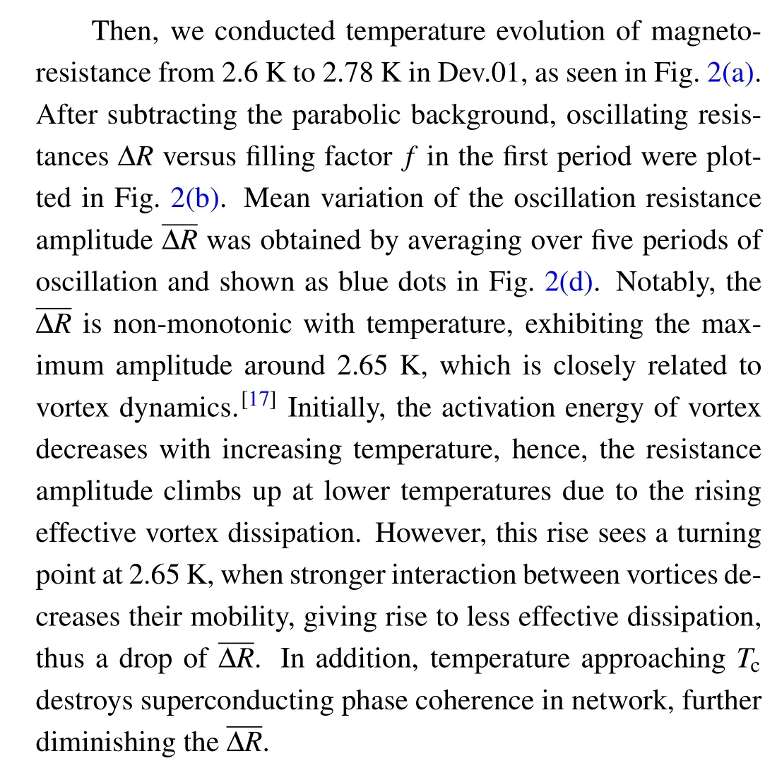
The as-grown 2D Mo2C crystals were transferred onto SiO2/Si substrates for device fabrication and electronic transport measurements. To avoid pinning effect at multi-domain boundaries,we selected rectangle and octagonal shaped samples with single domain.[30,31]Figure 1(a)shows the schematic of a standard four-terminal device of superconducting Mo2C crystalline square network and the electrical measurement setup. The electrodes were first fabricated by the standard electron-beam lithography (EBL) followed by electron-beam evaporation(EVE)of bilayer-metal Ti/Au=5/90 nm.Then we etched Mo2C channel crystals via the mask of electron-beam resist defined by another EBL process. The etching was conducted in an inductive coupled plasma(ICP)enhanced reactive ion etching (RIE) equipment, whose recipes include 300 W RF power,80 W ICP RF power,50 sccm CF4as main etchant,35 mTorr pressure and 30 s process time to ensure complete reaction of Mo2C crystal. Figure 1(b)shows a scanning electronic microscopy (SEM) image from a part of an etched Mo2C square-network sample Dev.01 with the inner loop size 400×400 nm2and the wire width 200 nm. The total number of unit square is 15×20=300. The low-temperature electrical transport measurements were conducted either in a physical property measurement system (PPMS) or a Dewar with variable temperature insert (VTI) equipment, cooling the sample down to 2 K with tunable magnetic field perpendicularly applied to the sample plane. An alternating current(AC)method using a lock-in amplifier at a low frequency of 17.777 Hz was employed with the driving current ranging from 10 nA to 100µA.
3. Results and discussion
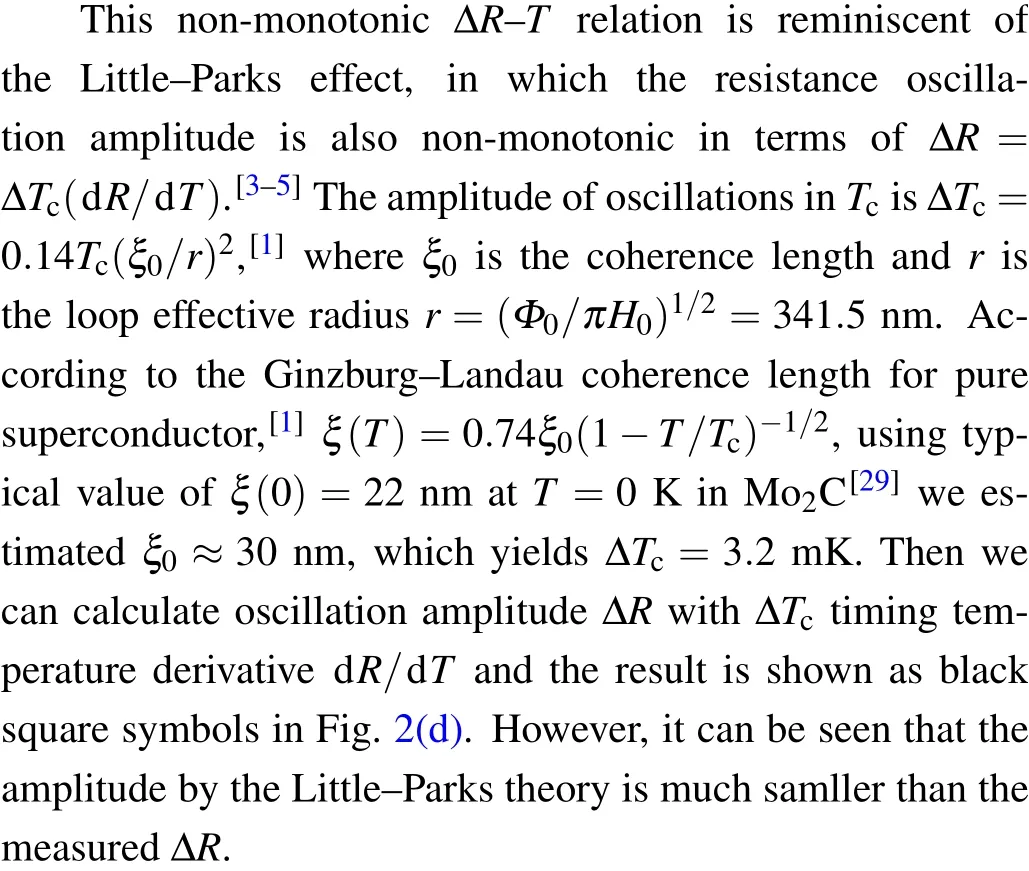
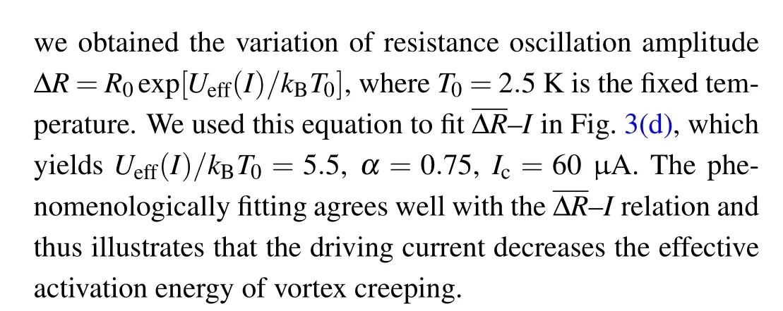
The inset of Fig. 1(c) shows resistance versus temperature with driving current 1 µA in Dev.01, from which superconducting transition can be observed. The critical transition temperatureTcis defined at which resistance equals 99%Rn,
whereRnis the normal state resistance,yieldingTc=2.96 K.The main panel of Fig. 1(c) shows the field dependence of the network resistance at 2.6 K, indicated by the green dot in the inset. We observed regular oscillations superposed on a parabolic background. This parabolic envelope stems from the contribution of the bulk of Mo2C strips.[5,13]The oscillating period isH0=56.5 Oe,corresponding to an effective loop area ofS=0.366 µm2, which is equivalent to the length of side 605 nm. Due to the finite widthw=200 nm in Mo2C strip, the equivalent length lies between the outer and inner boundaries for unit square. As shown by the white dashed box in Fig.1(b),the actual effective area circles along the middleline of the stripe,in reasonable agreement with the lattice parameter of the nano-patterned square network. Therefore,the periodic modulations pointed by black arrows are close to the Little-Parks effect,where each unit square is filled with integral multiple of vortices,leading to commensurate filling and forming an energetically stable lock-in state.[9]
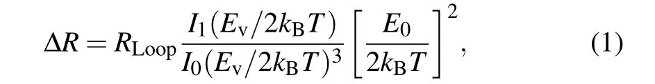
Figure 1(d) is a magnification of the first oscillating period in Fig. 1(c), shaded in light canary. The abscissa is reduced to filling factorf=H/H0and the parabolic background has been subtracted. As indicated by the arrows,well-defined dips are observed atf=1/3, 1/2, 2/3 and other fillings, in addition to the fundamental dip atf=±1. These dips at fractional fillings are associated with the commensurate arrangement of vortex-lattice with lower energy in the presence of underlying network.[33,34]Quantitatively, the phase boundaries are calculated in the spirit of mean-field theory by solving the linearized Ginzburg-Landau equation on the nodes.[9,10]This is analogous to the problem of an electron on a square lattice with unifrom magnetic field,whose energy spectrum is calculated in the tight-binding form by Hofstadter[35]and only the edge of the spectrum is related to superconducting-network problem.The factional fine structures in Fig.1(d)are in agreement with the theory[9]and previous expriments,[13]indicating the effective interaction between vortex-lattice and underlying crystalline Mo2C wire network.
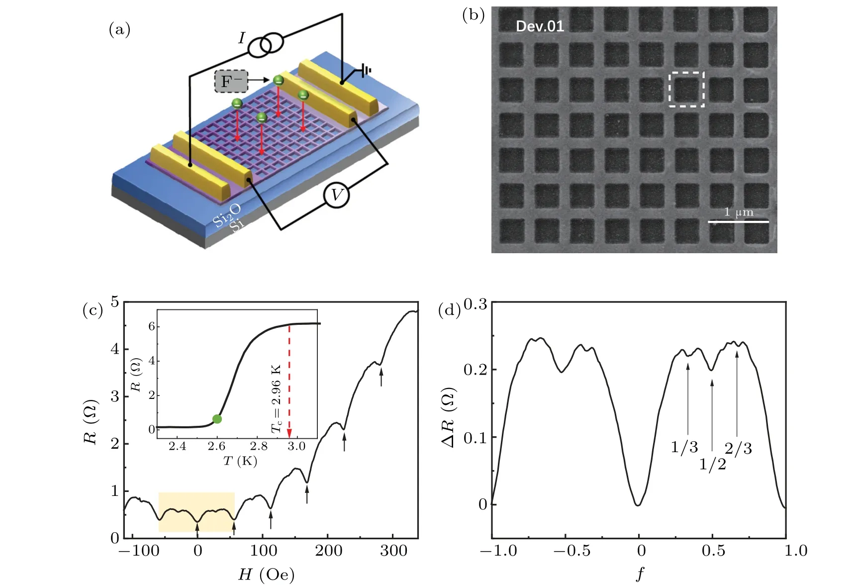
Fig.1. (a)Schematic of four-terminal device and its electrical measurement for finite superconducting square wire-network based on 2D crystalline Mo2C. The square network is fabricated by reactive ion etching with etchant CF4. Green dots represent fluorinion excited by plasma. (b) SEM image of a part of network channel in Dev.01. The white dashed box indicates the effective loop area. (c)Magnetoresistance at 2.60 K.The arrows indicate the magnetic field values corresponding to integral number of filling factor f =H/H0 per unit cell of the network. Inset shows resistance versus temperature with critical temperature Tc=2.96 K.(d)Magnified view of the first period(-H0 ≤H ≤H0)of the critical line. In addition to the fundamental dips at f =0 and±1,the secondary dips at f =1/3,1/2,2/3 are indicated by the corresponding arrows.
Recent study focusing on the amplitude anomaly proposed a model that the enhancement of ΔRis due to the interaction between thermally excited moving vortices and the oscillating persistent currents induced in the loops,[21,22]where the induced current is periodic stemming from the flux quantization,[2-5]with the derived ΔRas follows:
whereRLoopis the effective resistance from the loop,I1andI0are respectively the first-order and zero-order modified Bessel functions of the first kind,kBis the Boltzmann constant,Evis the energy needed for creation of the vortex/antivortex in a ring,E0is associated with the interaction between a vortex or an antivortex and the current. Specifically,Ev=Φ20ln[2w/πξ(T)]/8π2Λ(T), wherewis the annulus width,ξ(T)=0.74ξ0(1-T/Tc)-1/2is the Ginzburg-Landau coherence length[1]andΛ(T)=2λ(T)2/dis the Pearl penetration depth in a film of thicknessdwith the London penetration depth[1]λ(T)=λ0[1-(T/Tc)2]-1/2, andE0=Φ20ln[(r+w/2)/(r-w/2)]/8π2Λ(T).
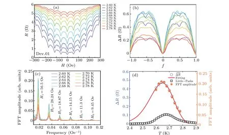
Fig. 2. (a) Resistance of the superconducting crystalline square-lattice as a function of magnetic field perpendicular to the sample plane at different temperatures from 2.6 K to 2.78 K.(b)Magnified view of the first period(-H0 ≤H ≤H0)of the critical line in(a)after subtracting a parabolic background. (c)FFT for ΔR-T in(b)from 2.6 K to 2.78 K.Amplitude peaks denoted by H1,H2,H3,H4,H5 and H6 correspond to oscillation periods of 56.5 Oe,28.24 Oe,18.87 Oe,14.15 Oe,11.3 Oe and 9.45 Oe,respectively,in line with the integral and fractional fillings in magnetoresistance. (d)Temperature dependence of the mean oscillation amplitude(blue circles)corresponds to y-axis on the left side. The red solid line is fitted with Eq. (1). The black squares show the resistance oscillations amplitude calculated for the Little-Parks effect. The orange snowflake symbols represent the amplitude of FFT for H1 corresponding to the y-axis on the right side.

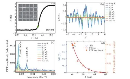
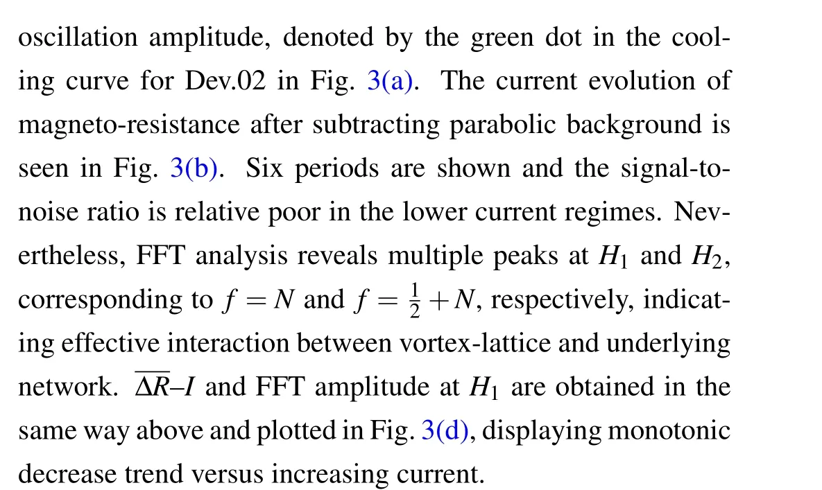
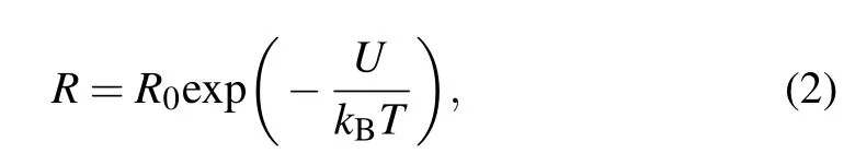
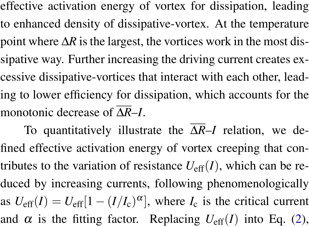
Fig.3. (a)Resistance versus temperature with the driving current 0.1µA for Dev.02. Inset: SEM image of a part of square-network channel.The white dashed box indicates the effective loop area.(b)Variation of resistance for the superconducting crystalline square-lattice as a function of magnetic field perpendicular to the sample plane with different driving currents from 0.5µA to 100µA.(c)FFT for ΔR-T in(b)from 0.5µA to 100µA.Amplitude peaks denoted by H1 and H2 correspond to oscillation periods of 66.56 Oe and 33.3 Oe, respectively, in line with the structures at f =N and 12 +N in magnetoresistance, where N is an integer. (d) Temperature dependence of the mean oscillation amplitude(blue circles)corresponds to y-axis on the left side. The red solid line is fitted based on a phenomenological model in the main text. The orange snowflake symbols represent the amplitude of FFT for H1 corresponding to y-axis on the right side.
In the presence of field, thermally assisted creeping of vortices over pinning energy barrier contributes to the dissipation,[1,36,37]which can be described by an Arrhenius activation law

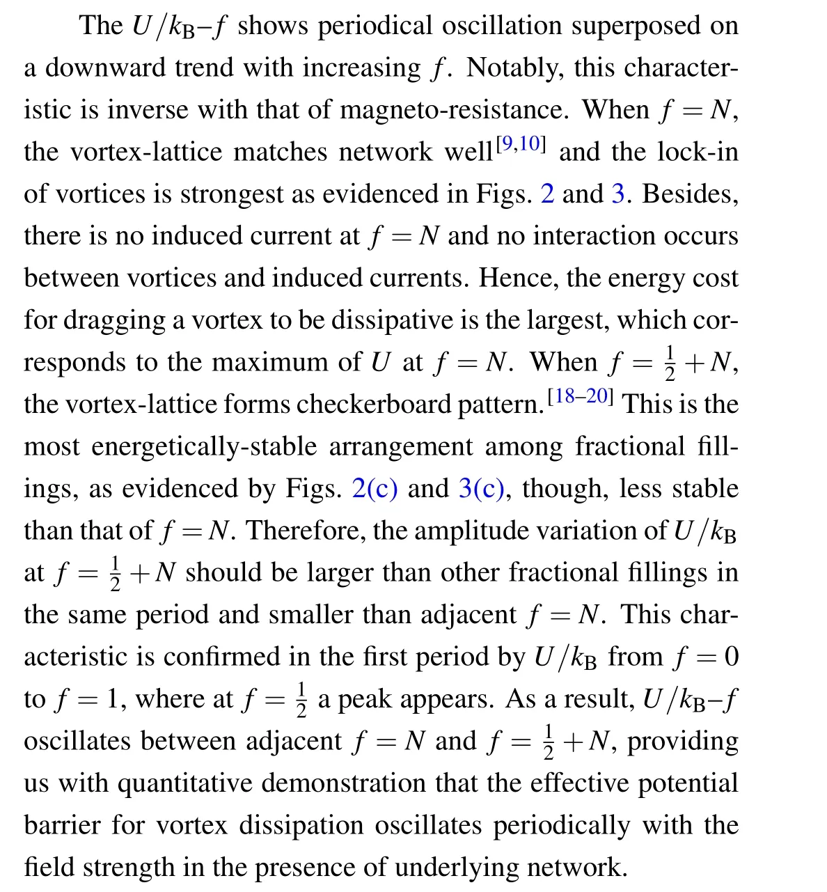
In continues and uniform 2D superconducting films,activation energy for vortex creep is observed to decrease monotonically with the applied magnetic field.[38,39]In contrast,in superconducting films nanopatterned into a network of loops,this activation energy becomes oscillatory, due to the periodic potential barrier by the network combined with the interaction between moving vortices and currents induced in nanoloops,[21,22]as we have shown in Fig. 2(d). The equivalent effective potential barrier for vortex motion can be analyzed in terms of Eq.(2).
Hence, to obtain the relation between effective potential barrier and field strength, we carried out measurement of resistance versus temperature under a series of magnetic field strength,as seen in Fig.4(a),with the driving current of 5µA.The magnetic field gradually shiftsR-Tcurves to lower temperature, with the critical field at about 20H0. In Fig. 4(b),we show an Arrhenius plot of theR-Twith the same data in Fig. 4(a). The data exhibits clear thermal activation behavior just belowTc, indicated by straight black dashed lines. We then can deduce the effective potential barrier from the linear fits to the activated region shown in Fig.4(b),and the obtainedU/kBtogether with magneto-resistance are plotted in Fig.4(c)with the same reduced abscissaf.
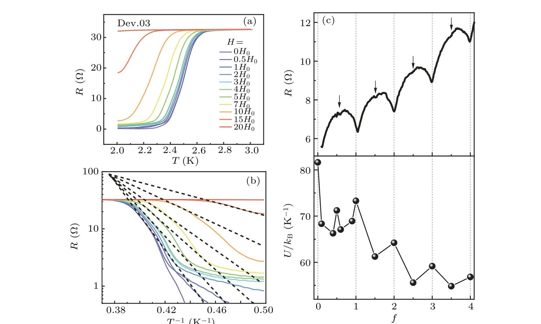
Fig.4. (a)Superconducting resistive transition of crystalline square-lattice Dev.03 at a series of fixed perpendicular magnetic fields. H0 is one integral oscillation period. (b) Arrhenius plot of the resistive transition in (a), indicating the thermally activated behavior. The black dashed lines are corresponding fitting curves using the collective flux creep model described by Eq.(2).(c)Magnetic field dependence of the activation energy U/kB (lower panel), which is obtained from fitting in(b). The upper panel shows the typical magnetoresistance. Note that the U/kB oscillates and matches well with the resistance structures.
4. Conclusion
To conclude, we have fabricated finite 2D superconducting square network based on crystalline Mo2C and observed resistance dips at both integral and fractional filling factors. The enhanced amplitude of resistance oscillation is attributed to interaction between thermally activated vortices and currents induced in the loops. Increasing the driving current declines activation energy for vortex, which in turn, leads to stronger vortex interaction and lower vortex mobility. The effective potential barrier for vortex dissipation oscillates periodically, synchronously and inversely with magneto-resistance in terms of underlying network. Our work demonstrates that the finite crystalline superconducting network based on Mo2C provides effective periodic potential barrier for vortex-lattice, and is a novel, clean and high-quality platform to study vortex arrangements and dynamics.
Acknowledgements
Project supported by the National Natural Science Foundation of China (Grant Nos. 11974026, 11774005, and 51802314),the National Key Research and Development Program of China(Grant No.2017YFA0303304),Science Foundation of Jihua Laboratory (Grant No. 2021B0301030003-03), and the Strategic Priority Research Program of Chinese Academy of Sciences(Grant No.XDB30000000). Dr. C.Xu acknowledges the support of the Youth Innovation Promotion Association of Chinese Academy of Sciences.
猜你喜欢
宝藏(2022年3期)2022-08-01
宝藏(2022年1期)2022-08-01
内燃机工程(2021年5期)2021-10-19
小学生作文辅导(2021年9期)2021-04-14
江苏教育·书法教育(2021年3期)2021-01-17
宝藏(2021年11期)2021-01-01
宝藏(2021年11期)2021-01-01
中成药(2017年4期)2017-05-17
学生天地·初中(2014年3期)2014-04-10
创新作文·低幼版(2013年1期)2013-02-04
- Chinese Physics B的其它文章
- Characterizing entanglement in non-Hermitian chaotic systems via out-of-time ordered correlators
- Steering quantum nonlocalities of quantum dot system suffering from decoherence
- Probabilistic quantum teleportation of shared quantum secret
- Spin–orbit coupling adjusting topological superfluid of mass-imbalanced Fermi gas
- Improvement of a continuous-variable measurement-device-independent quantum key distribution system via quantum scissors
- An overview of quantum error mitigation formulas