
Light-modulated graphene-based φ0 Josephson junction and-φ0 to φ0 transition
2024-02-29 09:19RenxiangCheng程任翔MiaoYu于苗HongWang汪洪DeliangCao曹德亮XingaoLi李兴鳌FenghuaQi戚凤华andXingfeiZhou周兴飞
Chinese Physics B 2024年2期
Renxiang Cheng(程任翔), Miao Yu(于苗), Hong Wang(汪洪), Deliang Cao(曹德亮),Xingao Li(李兴鳌),†, Fenghua Qi(戚凤华), and Xingfei Zhou(周兴飞),§
1New Energy Technology Engineering Laboratory of Jiangsu Province,School of Science,Nanjing University of Posts and Telecommunications,Nanjing 210023,China
2School of Electronic and Information Engineering,Jinling Institute of Technology,Nanjing 211169,China
3School of Electronic Engineering,Nanjing Xiaozhuang University,Nanjing 211171,China
Keywords: graphene,circularly polarized light,staggered sublattice potential,ϕ0 Josephson junction
1.Introduction
Graphene, a flat monolayer of carbon atoms arranged in a two-dimensional (2D) honeycomb lattice, was studied theoretically in 1947.[1]It was viewed as a thriving theoretical toy model until the realization of graphene in experiment in 2004.[2]By using the tight-binding model, there are two inequivalent cornersKandK′in the first Brillouin zone,around which is a conical band structure described by the massless Dirac equation.[3]Owing to its linear electronic spectrum,graphene has become a new type of “relativistic” material,where some unobservable relativistic phenomena in high energy physics, such as Klein tunneling and anomalous Klein tunneling,[4–8]can be easily mimicked and tested in condensed matter physics.Graphene not only provides a highly practical and prospective platform for studying fundamental physics, such as half-integer quantum Hall effect,[9]specular Andreev reflection,[10]topological phase transition,[11–14]and superconductivity,[15–18]but also has extraordinary applications in future, such as next-generation electronics and photonics,[19,20]device physics,[21]and heterostructure.[22]With the rise of graphene, the research about two dimensional materials, such as silicene,[23]2D transition metal dichalcogenides,[24–26]and phosphorene,[27,28]flourishes and continues to provide a fertile ground for applications such as energy storage and novel topological electronic devices.[29–31]
Josephson effect, the flow of supercurrent between two pieces of superconducting material separated by a thin layer of insulating material, was first predicted by English physicist Josephson and then was verified in experiment by Anderson and Rowell.[32,33]In this case, the minimal Josephson free energy appears at zero phase difference by calculating the phase-difference-dependent Josephson free energy,which is called 0 Josephson junction.When the insulating material is replaced by a ferromagnetic metal,i.e.,superconductorferromagnet-superconductor junction, the minimal Josephson free energy may appear atπphase difference and the direction of the critical supercurrent may be reversed, which is called 0–πtransition and is suggested as a promising device to realize qubits.[34–36]When the minimal Josephson free energy appears atϕ0phase difference (ϕ0̸= 0,π),the finite supercurrent exists at zero phase difference.This Josepshon junction calledϕ0Josephson junction with an unconventional supercurrent-phase relationJ=Jcsin(φ-ϕ0),which was discussed in the nanowire-based Josephson junction applied by the Rashba spin–orbit coupling and the Zeeman field,[37,38]the magnetic field-modulated quantum spin-Hall insulator,[39]the one-dimensional topological interface states constructed in a 2D honeycomb-lattice system,[40]the magnetized topological insulator interfaces,[41]the electrically modulated silicene nanoribbon,[42]a Bi2Se3-based Josephson junction in the presence of an in-plane magnetic field,[43]and the quantum anomalous Hall insulator.[44]These Josephson junctions play an important role in the design of superconducting circuits,[45–48]which stimulates researchers to study the Josephson effect constantly.
The graphene-based Josephson junction was studied widely.[49–54]The bipolar supercurrent in graphene was observed.[50]AπJosephson junction was predicted.[51]The PbIn–graphene–PbIn Josephson junction would facilitate the development of superconducting quantum information devices.[52]Supercurrent rectification effect in graphenebased Josephson junctions was discussed.[53]Electric controlledϕ0Josephson junction was investigated in twisted bilayer graphene in theory.[54]However, the realizations of topological edge states-inducedϕ0Josephson junction in graphene were rare.Although the edge states-inducedϕ0Josephson junction were discussed in silicene and other 2D materials,[40,42,44]the realization of superconductivity in graphene is easier than the one in this materials experimentally.So, in this work, we discuss how to realize topological edge states-inducedϕ0Josephson junction in graphene.The schematic diagrams for graphene-based Josephson junction is shown in Fig.1.The chiral edge states is induced by the offresonant circularly polarized light,which was studied in both theory and experiment.[55,56]The staggered sublattice potential induced by SiC substrate will modulate the chiral edge states in the middle region,[13]which is the key point for the realization ofϕ0Josephson junction.

Fig.1.Schematic diagram for graphene-based Josephson junction.The zigzag graphene nanoribbon is divided into three regions consist of two superconducting regions and a normal region.The superconductivity in left and right regions are realized by applying an s-wave superconductor.In the normal region, the graphene nanoribbon is deposited on an SiC substrate.The off-resonant circularly polarized light irradiates three regions.The chiral edges with spin degeneracy are shown in the middle region.
The paper is organized as follows.We firstly give the model and basic formalism.Then, the numerical results and theoretical analysis are presented and discussed.Finally, the main results of this work are summarized.
2.Models and methods
We consider a zigzag graphene nanoribbon which is deposited on an SiC substrate and irradiated by an off-resonant circularly polarized light.The Hamiltonian of the zigzag graphene nanoribbon is
The first term of Eq.(1) is the nearest-neighbor hopping of electron with the creation(annihilation)operator(ci(j))ati(j) site and the hopping integralt=2.82 eV.The symbols〈i,j〉and〈〈i,j〉〉represent nearest neighbors and next-nearest neighbors, respectively.The second term of Eq.(1) denotes the staggered sublattice potential term with the site energy∆and the sublattice indexµi=1(-1)for A(B)sublattice.The third term of Eq.(1) is the Haldane term which is induced by the off-resonant irradiation with the illumination parameter∆ω.η=1 (-1) represents the right (left) circularly polarized light.When the next-nearest-neighbor hopping is anticlockwise(clockwise)in the plane,the symbolνijis equal to 1(-1).
According to the tight-binding model,the energy bands of zigzag graphene nanoribbon with different parameters∆and∆ωare shown in Fig.2.The quantum anomalous Hall effect is induced by irradiating off-resonant left(right)circularly polarized light,shown in Figs.2(a)and 2(b).
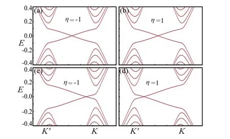
Fig.2.Dispersion relations of a zigzag graphene nanoribbon by irradiating off-resonant left(right)circularly polarized light for panels(a)–(c)((b)–(d)).(a)–(b)There is no SiC substrate.(c)–(d)There is an SiC substrate.The unit for energy is 1 eV and the width of nanoribbon W =60 atoms.
It is obvious that the light-induced edge states are independent of the polarization of light.But, when the staggered sublattice potential is considered,shown in Figs.2(c)and 2(d),the light-induced edge states are dependent on the polarization of light.The intersection of edge states moves toK(K′)valley when the left(right)circularly polarized light is irradiated on the zigzag graphene nanoribbon.In order to investigate the properties of edge states modulated by the cooperation of the off-resonant light and the staggered sublattice potential,the uniform Hamiltonian for top and bottom edge states is approximately given as[57,58]

In our system,shown in Fig.1,the electron and hole excitations are described by the Bogoliubov–de Gennes (BdG)equation
The wavefunctions of electron and hole in the middle regions are
In the short-junction regime, due to the continuity of wavefunction at interface, the wavefunctions in both middle and superconducting regions at interfaces are continuous, i.e.,rψ-SL|x=0=Ψ|x=0andtψ+SR|x=L=Ψ|x=Lin whichΨ=aψe+bψhandr,a,b, andtare the probability amplitudes of the corresponding wavefunctions.Obviously, whenr,a,b,andtare treated as four variables,there is a system of linear equations made up of four equations.In order to ensure the nonzero solution, the value of determinant of coefficients is equal to zero.Thus,we obtain
whereφ=φL-φRis the phase difference between left and right superconductors.From the above equation, it is easy to obtain (1/2)[(ke-kh)L-2β+φ]=nπwith integern.By some calculations,we can get
These levels are called Andreev bound state (ABS) levels which make the Cooper pair cross the normal region.
3.Results and discussion
3.1.Andreev bound state levels
In the short-junction regime, The ABS levels are calculated by Eq.(10)
It is obvious that the effective phase shift happens in the coaction of left(right)circularly polarized light and SiC substrate.The phase difference-ABS levels are shown in Fig.3.The ABS levels are symmetric about phase differenceφ=πwithout SiC substrate,shown in Figs.3(a)and 3(b).In other words,there is no phase shift in the presence of only polarized light.In addition,it is difficult to distinguish the effect of left circularly polarized light and right circularly polarized light from Figs.3(a)and 3(b).In the coaction of left(right)circularly polarized light and SiC substrate, shown in Figs.3(c) and 3(d),the effective phase shift happens and the directions of phase shift for two types of circularly polarized light are opposite,which aries from the fact that the direction of valley polarization is dependent on the polarized direction of light, shown in Figs.2(c) and 2(d).By using the values of parameters in Fig.3, the effective phase shift can be estimated by Eq.(11),i.e., 2[η(∆L/¯hv)mod2π]+π.It is easy to obtain that the effective phase shift is approximately equal to 2.6505 (3.6325)for left (right) circularly polarized light, which are well consistent with the numerical results in Figs.3(c) and 3(d).According to the periodicity of Eq.(11),the effective phase shift is approximately equal to 2[η(∆L/¯hv)mod2π)≈η0.488 for left (right) circularly polarized light, which indicates that the left circularly polarized light and the right circularly polarized light make the effective phase shift opposite completely.The effective phase shift will bringϕ0junction.
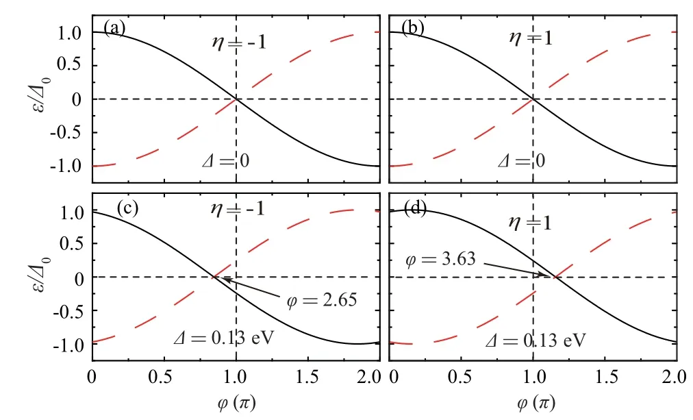
Fig.3.(a)–(d)Andreev bound state levels versus the phase difference with illumination parameter ∆ω =0.2 eV.The black (red-dotted) line denotes Eq.(11)with positive(negative)sign.The junction length L is 10 nm.
3.2.The ϕ0 junction and-ϕ0 to ϕ0 transition
According to Eq.(11), the relation between the Josephson currentJand the positive ABS levels at zero temperature is given as[59]
Figure 4 shows the Josephson current as a function of the phase difference.The shape of black line reveals the Josephson junction is a traditional 0 junction in the presence of offresonant circularly polarized light without substrate,which is consistent with the characteristic of ABS levels in Figs.3(a)and 3(b).In the coaction of off-resonant circularly polarized light and SiC substrate, from Eqs.(11)and(12), when phase differenceφ=0,
as cos(-η(∆L/¯hv))>0 (<0).By using the values of parameters in Fig.3, when the left (right) circularly polarized light is irradiated in Josephson junction,the Josephson current is approximately equal to 0.241(-0.241)as phase differenceφ=0,which is consistent with the numerical results in Fig.3 with red-dotted blue-dotted lines.This is the characteristic ofϕ0junction.By some simple calculations,it is easy to obtainϕ0=2η[(∆L/¯hv)mod2π]≈η0.488,which is consistent with the phase shift of ABS levels in Figs.3(c)and 3(d).
Figure 5 shows the Josephson current as a function of the illumination parameter∆ωwith the staggered sublattice potential∆=0.13 eV and phase differenceφ=0.The Josephson current displays a nondamped oscillation with variation of∆ω,which is consistent with Eq.(12)asφ=0.Interestingly,the behaviors of nondamped oscillation for left and right circularly polarized lights are opposite completely,which means that-ϕ0junction can be changed toϕ0junction by modulating the direction of polarization of light.This is similar to the traditional 0–πtransition.Thus,the transition phenomenon in Fig.5 is called as-ϕ0toϕ0transition,which is the generalization of 0–πtransition.It is easy to make-ϕ0toϕ0transition become 0–πtransition by adjusting the illumination parameter∆ωand the direction of polarization of light.
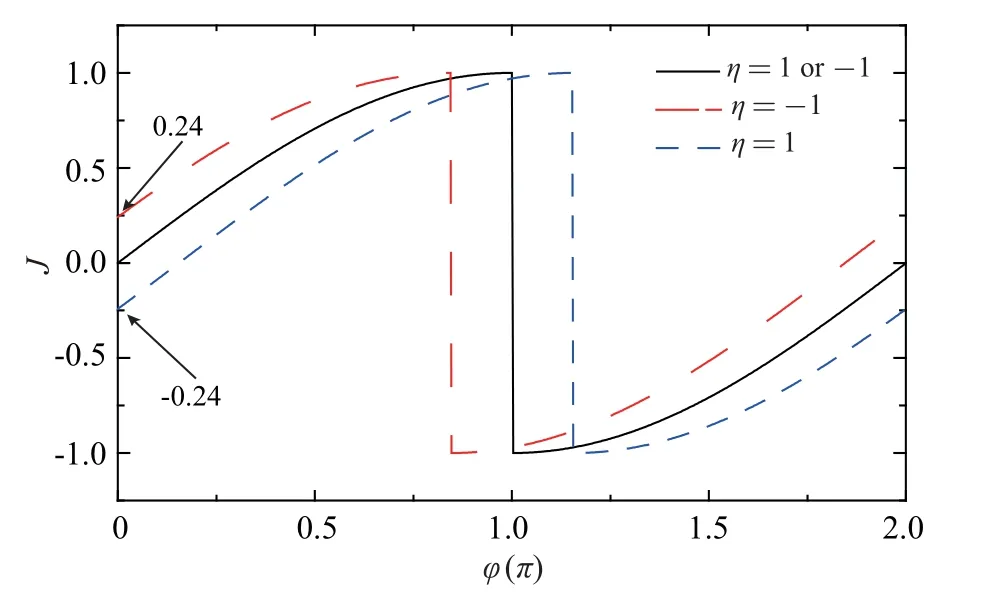
Fig.4.Phase difference-dependent Josephson current with illumination parameter ∆ω =0.2 eV.The black line denotes the case of left (right) circularly polarized light without substrate.The red–dotted(blue–dotted)line denotes left(right)circularly polarized light with SiC substrate-induced gap∆=0.13 eV.The unit for Josephson current is e∆0/¯h.The junction length L is 10 nm.

Fig.5.Illumination parameter-dependent Josephson current with ∆=0.13 eV and phase difference φ =0.The black(red–dotted)line represents the case of left (right) circularly polarized light.The unit for Josephson current is e∆0/¯h.The junction length L is 10 nm.
In order to clarify-ϕ0toϕ0transition clearly, we calculate the phase-dependent free energy of Josephson junction,[60]which is defined as
The position of minimal free energy decides the type of Josephson junction.The minimal free energy is atφ= 0 with∆ω=0.2 eV and∆=0, which is called 0 junction and shown in Fig.6 with black line.When the staggered sublattice potential is considered, shown in Fig.6 with red–dotted(blue–dotted) line, the minimal free energy is atφ= 0.49(-0.49) in the presence of right (left) circularly polarized light, which is well consistent with the analytical solution(ϕ0=2η[(∆L/¯hv)mod2π]≈η0.488)from Eq.(11).It is obvious to find that the type of Josephson junction transitions from 0.49 junction to-0.49 junction by changing the direction of polarization of light,shown in Fig.6,which is similar to the case that the type of Josephson junction transitions from 0 junction toπjunction(0–πtransition).So,the transition in our paper is called-ϕ0toϕ0transition,which generalizes the concept of 0–πtransition.The difference between these two types of transition is that the transition of Josephson current at zero phase difference is the signature of-ϕ0toϕ0transition(shown in Fig.5)while the critical current transition is the signature of 0–πtransition.

Fig.6.Phase-dependent free energy of Josephson junction with ∆ω =0.2 eV.The black line represents the case of left or right circularly polarized light without staggered sublattice potential.The red–dotted (blue–dotted)denotes the case of left(right)circularly polarized light with staggered sublattice(∆=0.13 eV).The unit for free energy is ∆0.The junction length L is 10 nm.
4.Conclusion
In conclusion,a light-modulated topological edge statesinducedϕ0junction is found in a graphene-based Josephson junction.In the nonsuperconducting region, the center ofmass wave vector of Cooper pair becomes finite and the opposite center of-mass wave vector to compensate is lacking in the coaction of the circularly polarized light and the staggered sublattice potential,which is the physical origin ofϕ0junction.In addition,by changing the direction of polarization of light,-ϕ0toϕ0transition is found,which generalizes the concept of traditional 0–πtransition.These results provide experimental proposals to realize graphene-basedϕ0Josephson junction and promise potential applications in phase-controllable Josephson devices.
Acknowledgements
Project supported by the National Natural Science Foundation of China (Grant Nos.12104232, 11805103, and 11804167), the Natural Science Foundation of Jiangsu Province,China(Grant Nos.BK20190137 and BK20180739),the Fundamental Research Funds for the Central Universities (Grant Nos.020414380195 and B230201042), the Jit-b Project(Grant No.201831),and the Natural Science Fund of Nanjing University of Posts and Telecommunications (Grant No.NY222163).
- Chinese Physics B的其它文章
- Unconventional photon blockade in the two-photon Jaynes–Cummings model with two-frequency cavity drivings and atom driving
- Effective dynamics for a spin-1/2 particle constrained to a curved layer with inhomogeneous thickness
- Genuine entanglement under squeezed generalized amplitude damping channels with memory
- Quantum algorithm for minimum dominating set problem with circuit design
- Protected simultaneous quantum remote state preparation scheme by weak and reversal measurements in noisy environments
- Gray code based gradient-free optimization algorithm for parameterized quantum circuit