
Angle-resolved photoemission study of NbGeSb with non-symmorphic symmetry
2024-02-29 09:19HuanMa马欢NingTan谭宁XuchuanWu吴徐传ManLi李满YiyanWang王义炎
Chinese Physics B 2024年2期
Huan Ma(马欢), Ning Tan(谭宁), Xuchuan Wu(吴徐传), Man Li(李满), Yiyan Wang(王义炎),
Hongyan Lu(路洪艳)5,†, Tianlong Xia(夏天龙)1,2,‡, and Shancai Wang(王善才)1,2,§
1Department of Physics,Key Laboratory of Quantum State Construction and Manipulation(Ministry of Education),Renmin University of China,Beijing 100872,China
2Beijing Key Laboratory of Opto-Electronic Functional Materials&Micro-Nano Devices,Renmin University of China,Beijing 100872,China
3School of Information Network Security,People’s Public Security University of China,Beijing 100038,China
4Institute of Physical Science and Information Technology,Anhui University,Hefei 230601,China
5School of Physics and Physical Engineering,Qufu Normal University,Qufu 273165,China
Keywords: non-symmorphic symmetry, nodal line, splitting of surface bands, angle-resolved photoemission spectroscopy
1.Introduction
Topological phases of matter witnessed significant advancements in recent decades.[1]These phases range from topological insulators to topological semimetals, including Dirac semimetals and Weyl semimetals.[2–4]The properties of these materials,such as dimensionality,degeneracy,slope,and the order of crossing in the bulk electronic structures,are governed by symmetry.[5]For instance,nodal points exist as zerodimensional entities at discrete points in the Brillouin zone(BZ), nodal lines manifest as one-dimensional features along specific lines in the BZ,and nodal surfaces characterize twodimensional(2D)structures found on particular planes in the BZ.Furthermore, the density of states (DOS) of low-energy excitations differs within these topological semimetals:nodalline semimetals exhibit a higher DOS for low-energy excitations along their nodal lines, while nodal-surface semimetals possess a constant DOS near the nodal surfaces.[5]
Materials with nonsymmorphic structures,such asWHMfamily (W= Zr, Hf, or La,H= Si, Ge, Sn, or Sb, andM=O, S, Se, and Te),[6,7]have been proposed to be nodal line semimetals in the absence of spin–orbit coupling(SOC).This characteristic makes them promising candidates in practical applications of 2D topological insulators for heterostructural devices.[8]ZrSiS, being the most representative among these materials,has been thoroughly studied and found to possess extraordinary properties.[9–14]For instance, in the field of quantum transport,ZrSiS demonstrates nonsaturating magnetoresistance (MR), butterfly shape angular MR with rotating magnetization, and nontrivial Berry phase extracted from the Shubnikov–de Haas (SdH) oscillations.[9,11]Moreover,several Dirac cones form a Fermi surface (FS) with Dirac nodes protected by non-symmorphic symmetry, allowing for the coexistence of surface states alongside bulk state bands in ZrSiS.[10,13]
NbGeSb shares the same structure of ZrSiS, and exhibits a wide range of properties.[15,16]The MR behavior of NbGeSb follows a parabolic trend, reaching an MR value of approximately 18% atT= 3 K andB= 14 T.[17]Angular MR measurements display a two-fold rotation symmetry.[18,19]Additionally, a negative MR has been observed in a magnetic field belowB=3 T.[19]Hall measurements reveal that electron carriers dominate the transport behavior.[17]Furthermore, the analysis of SdH oscillations demonstrates a nontrivial Berry phase,providing evidence for the topological nature of NbGeSb.[18]The slab model calculations showed that the Ge-terminated surface exhibits type-I and type-II Weyl points, while the Sb-terminated surface has only type-I Weyl point.[19,20]Another investigation focused on Nb-terminated slab models with varying numbers of layers(1,2,4,6)identified a quadruple degenerate node nearΓas well as a topologically protected Dirac cone.[21]
In ZrSiS,there exist surface states originating from Zr and S, respectively.However, they are separated in energy.The NbGeSb is the aliovalent substitutions of Nb for Zr and Sb for S.With the substitution,it provides a possibility to manipulate the electronic properties, such as shifting the surface bands to create a band inversion of the surface bands.Furthermore,with the substitution of heavy elements,e.g.,Sb for S,the SOC should be considered.Spin-polarized surface states have been reported on NbGeSb.[20]However,the detailed bulk state such as nodal lines needs to be studied with photon energy dependence,and the spin polarized surface states and band inversion deserve detailed investigation.
In this paper, we extend the investigation by utilizing both the soft x-ray and ultraviolet photon to study both the bulk states and surface states band structures of NbGeSb.We employ angle-resolved photoemission spectroscopy(ARPES),in conjunction with density functional theory (DFT) calculations and slab models of the bulk and surface states, to gain a comprehensive understanding of the electronic properties of NbGeSb.We separate the surface state from bulk state, and identify the existence of nodal lines.We find the Rashiba-like splitting of the surface states and the Weyl-like crossings, as well as an asymmetric gap opening.
2.Crystal structure
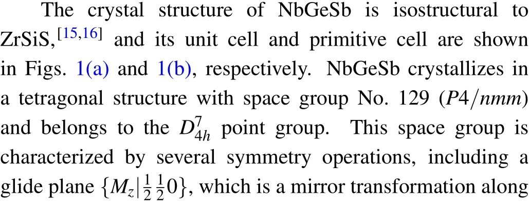
Fig.1.Crystal structure of NbGeSb with space group P4/nmm(No.129, D74h).(a) Unit cell.(b) Primitive cell.The upper row and lower row are top view and side view,respectively.
3.Methods
High quality single crystals of NbGeSb were grown by chemical vapor transport method.[17,18]Firstly,polycrystal of NbGeSb was prepared by the solid-state reaction.The mixtures of Nb, Ge and Sb powder were sealed in a quartz tube with a ratio of 1:1:1 and heated to 800◦C.Secondly,10 mg/cm3of I2was used as transport agent to grow single crystals, and the temperature gradient was set as 950◦C–750◦C.The growth of single crystal was carried out in a twozone furnace and lasted for three weeks.
ARPES measurements were performed at the Dreamline 09U beamline of Shanghai Synchrotron Radiation Facility(SSRF) that is equipped with Scienta-Omicron DA30L electron analyzer, beamline 13U of National Synchrotron Radiation Laboratory (NSRL) in Hefei and at Renmin University of China (RUC) both of which are equipped with Scienta-Omicron DA30 electron analyzers.The samples were cleavedin situ.During the measurements, the temperature was kept lower thanT=36 K,the vacuum was maintained better than 8×10-11Torr, and the energy resolution was set better than 15 meV.
The electronic structure was studied by the first-principles calculations with the projector augmented wave (PAW)method[24,25]as implemented in the VASP package.[26–28]For the exchange–correlation function, the generalized gradient approximation(GGA)of the Perdew–Burke–Ernzerhof(PBE)formula[29]was adopted.The kinetic energy cutoff of the plane-wave basis was set to be 500 eV.The width of the Gaussian smearing method was 0.01 eV.The relaxation was stopped when the change of the total energy was smaller than 10-4eV(10-5eV)between two ionic steps for bulk(slab)calculations,and the energy convergence criterion was 10-11eV(10-6eV) for bulk (slab) calculations.A 26×26×12Γcenteredk-point mesh was utilized for the bulk BZ sampling while a 18×18×1 for the slab BZ sampling.For slab calculations,five slab models along thec-axis with 1 to 5 layers were constructed,more than 20 ˚A vacuum thickness was adopted to eliminate the interactions of neighboring layers.The termination plane of slab models is the Sb atomic layer.
The crystal structure is visualized in the VESTA software.[30]Thek-point mesh was generated by the VASPKIT software for the FS calculation,[31]and FSs are visualized in the FermiSurfer software.[32]The atomic-projection band structure is shown by the pymatgen code.[33–35]The primitive BZ and 2D BZ of the projected(001)surface of NbGeSb are shown in Fig.2(b).For simplicity,we useΓ,X,M,etc.in the 3D BZ,whileΓ,X,Mnotations in the 2D BZ.
4.Results
4.1.Nodal lines and nodal surfaces
The calculated bulk band structures of NbGeSb without and with SOC are depicted by black and red lines, respectively, in Fig.2(a).A Dirac linear dispersion (i.e., a node),indicated by a green circle,is observed nearEFalong theΓ–Xdirection.This Dirac node is protected by theC2vsymmetry alongΓ–Xline, a characteristic shared with similar materials like ZrSiS.[10]The Dirac node further forms a nodal line alongkzdirection and at thekz=0 andkz=πplanes in the BZ,forming a closed loop,as depicted by red dashed lines in Fig.2(b).When taking SOC into account, a small gap opens at the node because theC2vgroup allows only one irreducible representation,[10]as depicted by the red lines inside the green circle in Fig.2(a).
In addition,as indicated by green square in Fig.2(a),two bands are degenerate at energyE-EF∼-1.15 eV at the highsymmetry pointX,which is protected by the non-symmorphic symmetry of the space group.[10]As presented by the black line in the figure, this degeneracy persists along theX–Mdirection.Additionally,as depicted by the red arrow in Fig.2(c),the node undergoes variations in binding energy at differentkzplanes, ranging fromkz=0 tokz=π.By analyzing the band dispersion alongX–Mdirections at differentkzplanes,this Dirac-crossing forms a nodal surface at the BZ boundary, i.e., at thekx=πplane (indicated by the green plane in Fig.2(b))and theky=πplane.[10,14]When the SOC is considered,the degeneracies alongX–Mdirections are lifted except at the high symmetry pointX,as indicated by the red lines in Fig.2(a).The nodal surfaces at thekx,y=πplanes transform into a nodal line along theX–Rdirection,as illustrated by the magenta line in Fig.2(b).
4.2.Band structure with different photon energies
To examine the band dispersion of NbGeSb, we conducted ARPES measurements using several typical photon energies.The FSs and band dispersion along high symmetry lines are shown in Fig.3.For comparison,a 3-layer slab calculation of FS topology and band dispersion with SOC is overlaid as solid curves on the top of the ARPES data.
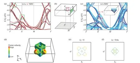
Fig.2.(a)Calculated bulk band structure of NbGeSb without(w/o)and with(w/)SOC(black and red lines,respectively).Green circle indicates Dirac linear dispersion,and green square indicates node at X.(b)Primitive BZ(upper panel),and 2D BZ of the projected(001)surface(lower gray shaded areas).Without SOC,the locations of the nodal lines and nodal surfaces are labelled by red dashed lines and green planes.With SOC,the locations of the nodal lines are labelled by magenta lines.For simplicity,only 1/8 part of these are labelled in BZ.(c)Calculated bulk band structure without SOC along k-lines in the inset of BZ.Lines with colors from black to light cyan represent k-lines in different kz-planes from kz=0 to kz=π.Red arrow indicates the node atX shifts to lower binding energy from kz=0 plane to kz=π plane.(d)Calculated bulk FSs of NbGeSb without SOC.FSs at(e)kz=0 plane and(f)kz=0.6π plane.Colors on FSs represent the Fermi velocity.
Compared with the calculated FSs of NbGeSb in Figs.2(d)–2(f), the FSs measured with photon energies of 412 eV and 100 eV in Figs.3(b)and 3(c)are more consistent with those of thekz=0 andkz=0.6πplanes, respectively.In Fig.3(b) with high photon energy of 412 eV, the FSs of surface states mainly exist around theΓpoint, while the FSs around theXpoint have much weaker intensity.In comparison, ARPES with low photon energy of 100 eV reveals that the FSs around theXpoint have stronger intensity, as shown in Fig.3(c).According to the universal curve of the photoelectrons’ inelastic mean free path in Fig.3(a), the photon is bulk sensitive at high energy of 412 eV, while it is surface sensitive at the energy of 20–100 eV.Combining the intensity variation with photon energy around theXpoint,the DFT band structures at differentkzplanes in Fig.2(c),and the slab calculations, we identify that the FSs around theXpoint are surface states.A high resolution mapping with photon energy of 20.5 eV is shown in Fig.3(d).The surface states around theXexhibit two clear elliptical shapes, which agrees well with the slab calculations.
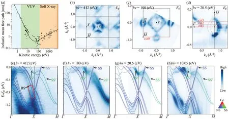
Fig.3.(a) The universal curve of the photoelectrons’ inelastic mean free path as a function of kinetic energy above the Fermi level.[22,23](b)–(d) FSs measured with hν =412 eV, 100 eV, 20.5 eV, respectively.(e)–(h) Band dispersions along theΓ–X–M line, measured with hν =412 eV, 100 eV, 20.5 eV, 10.05 eV, respectively.Surface bands SS originating from Nb 4d-orbitals are labelled by blue color, while surface bands SS′ originating from Sb 5p-orbitals are labelled by green color.Red rectangle in (e) indicates the bands of bulk states (BS)measured with bulk sensitive high photon energy.For comparison,the 3-layer slab calculation with SOC is overlaid as solid curves on the top of the ARPES data.Calculated FSs are indicated by black curves,and calculated band structures are atomic projection.
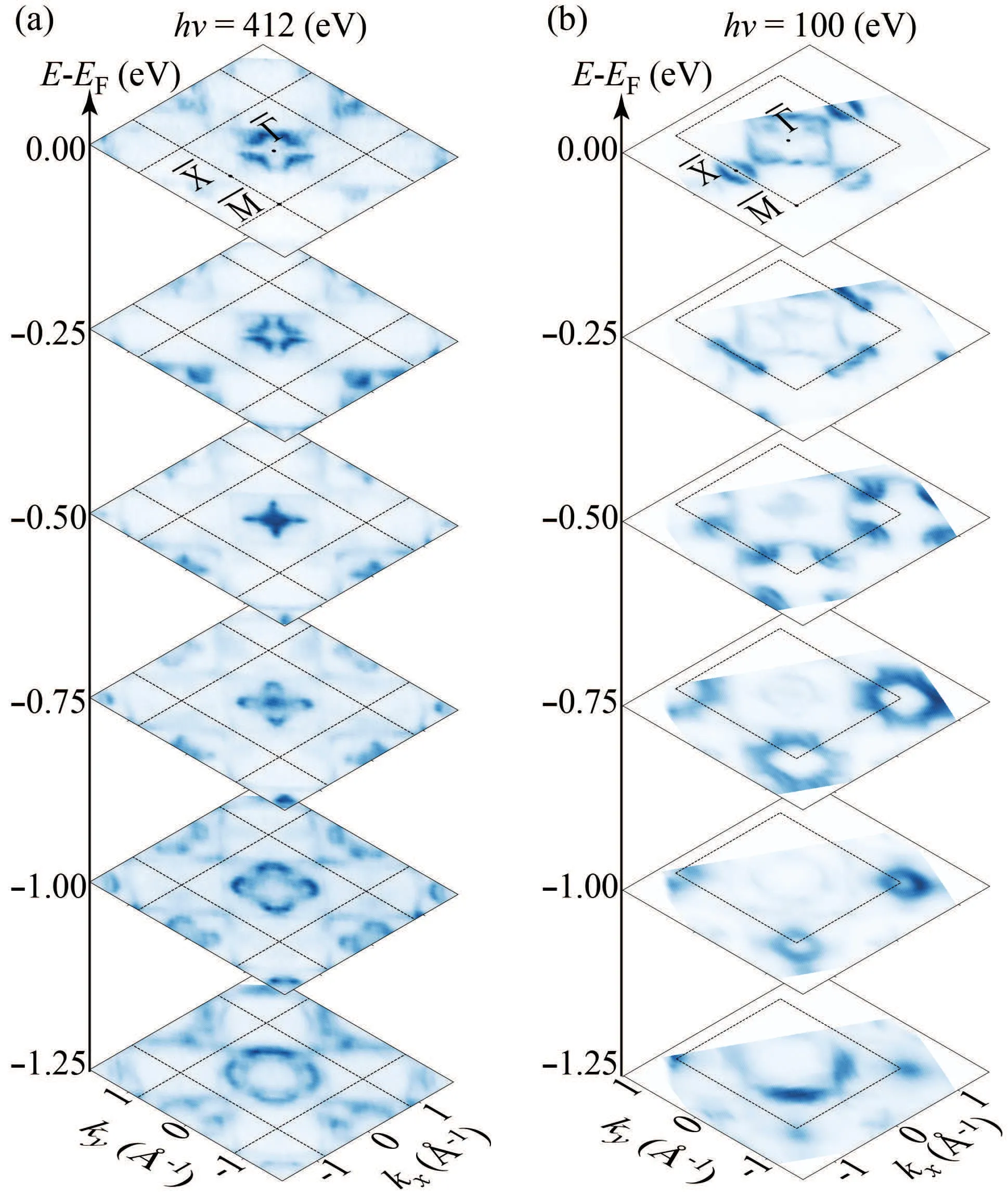
Fig.4.Constant-energy ARPES intensity plots with (a) hν =412 eV and(b)100 eV,measured at energies from EF to E-EF=-1.25 eV.
To enhance the contrasts,constant energy intensity maps at various binding energies were obtained at photon energies ofhν=412 eV and 100 eV,as shown in Fig.4.These maps reveal distinct features at different binding energies.At lower binding energies,particularly nearEF,the contrast is evident,showcasing the existence of surface states near theXpoint athν=100 eV,as well as the different intensity patterns at the BZ center.As we move to higher binding energies, e.g., approximately 1.25 eV belowEF, the surface states vanish and the constant energy plots of these two photon energies become more consistent.
Figures 3(e)–3(h)present the band dispersions along the high symmetry linesΓ–X–M, measured with different photon energies:hν=412 eV, 100 eV, 20.5 eV, and 10.05 eV,respectively.In Fig.3(e) with bulk sensitive high photon energy of 412 eV,the bulk bands nearΓpoint are clearly visible with high intensity.Conversely, the bands of surface states have much weaker intensity atXpoint and alongX–Mdirection,where the blue and green calculated surface states bands are present.Notably, linear dispersions are observed in the red rectangle in Fig.3(e), where the bulk bands exist in calculations.These linear dispersions form a node atXpoint,in agreement with the bulk calculations in Fig.2(a).To confrim this bulk state node, we conducted measurements with a range of high photon energies fromhν=335 eV to 495 eV,and show the integrated intensity atEFas a function of the photon energy–k‖in Fig.5(a).This intensity map shows a three-dimensional (3D) FS in thek‖–kzplane, indicating the bulk nature of these bands.Figure 5(b)provides confrimation of the bulk state nodes at theXpoint.These nodes are observed with photon energies ranging from 335 eV to 365 eV,and the variation of the Dirac-crossing in energy offers an evidence of the existence of the bulk nodal line alongX–R, as indicated by the magenta lines in Fig.2(b).At a photon energy of 10.05 eV,which is also bulk sensitive according to the universal curve, the enhancement of the bulk states and the suppression of the surface states are clearly seen in Fig.3(h).In comparison, the surface states are clearly visible with enhanced intensity athν=100 eV and 20.5 eV,as demonstrated in Figs.3(f)and 3(g).
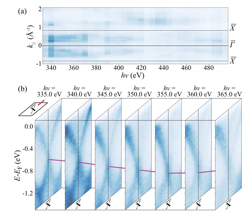
Fig.5.(a)The photon energy–k‖ intensity map along theΓ–X plane in BZ.(b) Band dispersions with different photon energies along the red line shown in inset of BZ.Magenta lines indicate nodal line alongX–R.
4.3.Surface state band splitting
According to the atomic-projection of band dispersions from slab calculation,the surface bands SS originate from Nb 4d-orbitals,while the surface bands SS′originate from Sb 5porbitals.Sharing the same structure with ZrSiS and with aliovalent substitution of Nb for Zr and Sb for S, NbGeSb hosts symmetry protected nodal lines and corresponding surface states that are similar to ZrSiS.[10]In ZrSiS,the surface state SS originating from Zr locates at energyE-EF∼-0.4 eV,while the surface state SS′originating from S locates at energyE-EF∼-1.7 eV.[13]In NbGeSb,due to the fact that Sb has one less valence electron than S,while Nb has one more electron than Zr,the corresponding surface state bands SS and SS′in NbGeSb shift toward each other.Eventually, these bands cross each other, resulting in a band inversion, and form the band crossings in the vicinity ofEF,as shown in Fig.3(f).
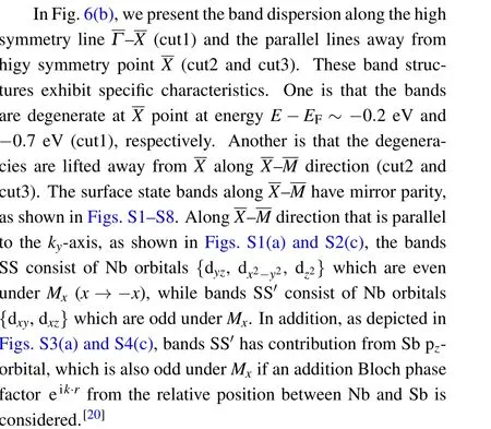
Now we focus on the band structure aroundXpoint.We present the experimental band dispersion along cut0–cut3 in Figs.6(a) and 6(b), and the calculated 3D surface state band dispersion in Fig.6(c).By extracting the peak position alongX–M(indicated by the blue and green dots)in Fig.6(a),clear band splittings of SS and SS′are observed.This observation is consistent with the slab calculations,which are overlayed as green and blue solid lines.From the atomic orbital-projection DFT calculations presented in Figs.S1–S8, the surface state bands arise predominantly from the outermost Sb layer and the top Nb layer.Additionally, by comparing DFT calculations of slab models with different layers, without and with SOC,in Fig.S9,we fnid that the SOC is crucial in producing the observed band splittings,while simply increasing the number of stacked layers can not drive the splitting of the bands in the slab models.
Such mirror symmetry observed in the electronic band structure is also reflected in spin textures.We calculate the spin textures corresponding to bands #3 and #4 in Fig.6(a),and display them in Figs.6(d) and 6(e).Along several high symmetry lines with mirror symmetry,Γ–X,X–M, andΓ–M, the spin textures are perpendicular to these mirror lines,as shown in Fig.6(d).Furthermore, as shown in Fig.6(e),the inner FS and the outer FS around theXpoint exhibit opposite spin polarizations.This observed surface state band splitting, together with the calculated spin textures, could be attributed to the Rashba-like splitting, which is caused by a space-inversion-symmetry breaking at the surface.[20,36]In comparison,Rashba-like splitting is negligible in ZrSiS,probably due to the lighter atomic mass of S than that of Sb in NbGeSb and the resultant smaller SOC in ZrSiS.[10,13,37]
As shown in the lower panel of Fig.6(c), after Rashbalike splitting, there are four crossings (labeled as c1 to c4).Considering the spin textures, crossings c2 and c4 occur between bands with the same spin polarization, while crossings c1 and c3 occur between bands with opposite spin polarizations.One of these mirror protected crossings c4 exhibits a band inversion between the spin-polarized states, resulting in a Weyl-like crossing.This band inversion is caused by the intrinsic band inversion of surface state.Analysis through the tight-binding model,with consideration of the spin–orbital interaction, reveals that at crossing c1, the change in spin between the bands is opposite to their change in orbital angular momentum.As a result, a gap opens at this crossing.[20]However,at crossing c3,the change in spin between the bands aligns with their change in angular momentum,resulting in a negligible gap.[20]try lineX–R, and the existence of surface states originating from Nb and Sb atoms.In comparison with ZrSiS,the surface bands shift toward each other, eventually crossing and causing a band inversion.We observe splitting of surface bands which could be attributed to the Rashba-like SOC,caused by space-inversion-symmetry breaking at the surface.The analysis of spin polarization projections reveals asymmetric gaps among band crossings, and the formation of Weyl-like points protected by mirror symmetry.NbGeSb provides a unique platform for studying the topological and symmetry-protected band inversion of surface state,contributing to our understanding of the electronic properties of this material.
5.Conclusion
In summary, we investigate the electronic structure of NbGeSb by using ARPES and DFT bulk and slab calculations.By using different photon energies and DFT calculations, we identify the existence of bulk nodal line along high symme-
Acknowledgements
Project supported by the National Key Research and Development Program of China(Grant No.2022YFA1403803).H.M.is supported by the Fundamental Research Funds for the Central Universities, and the Research Funds of Renmin University of China (Grant No.22XNH099).The results of DFT calculations described in this paper are supported by HPC Cluster of ITP-CAS.M.L.is supported by the National Natural Science Foundation of China (Grant No.12204536),the Fundamental Research Funds for the Central Universities,and the Research Funds of People’s Public Security University of China (PPSUC) (Grant No.2023JKF02ZK09).T.L.X.is supported by the National Key R&D Program of China (Grant No.2019YFA0308602) and the National Natural Science Foundation of China (Grant Nos.12074425 and 11874422).Y.Y.W.is supported by the National Natural Science Foundation of China (Grant No.12104011).H.Y.L.is supported by the National Natural Science Foundation of China (Grant No.12074213), the Major Basic Program of Natural Science Foundation of Shandong Province (Grant No.ZR2021ZD01),and the Project of Introduction and Cultivation for Young Innovative Talents in Colleges and Universities of Shandong Province.

- Chinese Physics B的其它文章
- Unconventional photon blockade in the two-photon Jaynes–Cummings model with two-frequency cavity drivings and atom driving
- Effective dynamics for a spin-1/2 particle constrained to a curved layer with inhomogeneous thickness
- Genuine entanglement under squeezed generalized amplitude damping channels with memory
- Quantum algorithm for minimum dominating set problem with circuit design
- Protected simultaneous quantum remote state preparation scheme by weak and reversal measurements in noisy environments
- Gray code based gradient-free optimization algorithm for parameterized quantum circuit