
Growth and characterization of Bi(110)/CrTe2 heterostructures:Exploring interplay between magnetism and topology
2024-02-29 09:17ZhenyuYuan袁震宇FazhiYang杨发枝BaiqingLv吕佰晴YaoboHuang黄耀波TianQian钱天JinpengXu徐金朋andHongDing丁洪
Chinese Physics B 2024年2期
Zhenyu Yuan(袁震宇), Fazhi Yang(杨发枝), Baiqing Lv(吕佰晴), Yaobo Huang(黄耀波),Tian Qian(钱天), Jinpeng Xu(徐金朋),6,7,†, and Hong Ding(丁洪),6
1Beijing National Laboratory for Condensed Matter Physics,Institute of Physics,Chinese Academy of Sciences(CAS),Beijing 100190,China
2School of Physical Sciences,University of Chinese Academy of Sciences,Beijing 100190,China
3Tsung-Dao Lee Institute and School of Physics and Astronomy,Shanghai Jiao Tong University,Shanghai 200240,China
4Shanghai Synchrotron Radiation Facility,Shanghai Advanced Research Institute,Chinese Academy of Sciences,Shanghai 201204,China
5Songshan Lake Materials Laboratory,Dongguan 523808,China
6CAS Center for Excellence in Topological Quantum Computation,University of Chinese Academy of Sciences,Beijing 100190,China
7School of Physics,Shandong University,Ji’nan 250100 China
Keywords: bismuth (110), chromium ditelluride (CrTe2), topological states, scanning tunneling microscopy(STM)
1.Introduction
Condensed matter physics has witnessed remarkable advancements driven by evolutionary concepts.[1]The discovery of the KT phase transition[2]and the integer and fractional quantum Hall effect[3,4]ignited a surge of interest in studying topological states of matter in condensed matter physics.To date, numerous topologically non-trivial materials have been predicted,[5–7]solidifying the research of topological states of matter as a notable frontier and hotspot within the field.The distinctive“bulk–boundary correspondence”in topological quantum matter offers immense potential for various applications,such as nondissipative transport enabled by topological protection.
Bismuth has long been a focal point of research due to its robust spin–orbit coupling and layer-dependent energy bands.Recent experiments and theories have suggested that bulk bismuth may possess characteristics of a high-order topological insulator,[8–10]albeit with some potential disputes.[11]Furthermore,two-dimensional(2D)topological insulators are more practical than their three-dimensional(3D)counterparts due to their one-dimensional (1D) nondissipative conductive channels.Currently, several 2D topological insulators have been discovered,such as HgTe/CdTe quantum wells,[12]InAs/GaSb/InAs triple quantum wells,[13]Bismuthene on an SiC substrate,[14]monolayer 1T′-WTe2,[15,16]and so on.However, comprehensive experimental evidence[17–23]supports that a 2D bismuth film can exhibit properties of a 2D topological insulator.Thus, further detailed experimental explorations are highly anticipated to shed light on this exciting area of research.Undoubtedly, bismuth is a material that exhibits a rich variety of topological states,and its combination with magnetism presents an exceptionally enticing direction.Additionally, in recent years, heterojunctions formed by coupling topological insulators with other materials have revealed a host of surprising physical phenomena.For example, the heterojunction formed by combining Bi2Te3and NbSe2exhibits properties of topological superconductivity,[24–26]while the coupling of FeTe and Bi2Te3in a heterojunction demonstrates interfacial superconductivity.[26–28]Therefore, exploring the physical properties of heterojunctions between topological insulators and other materials holds immense value in unraveling potential physical phenomena.In summary, exploring the convergence of topologically diverse materials,like bismuth, with magnetism, and investigating heterojunctions between topological insulators and other substances,offer intriguing avenues of research with significant potential for discoveries.
In recent years,there has been a multitude of 2D magnetic materials that have been discovered which are particularly attractive due to their potential application value in atomiclevel spintronic devices.[29–35]CrTe2is a rare magnetic material that surprisingly maintains its ferromagnetism at room temperature.[36–39]Additionally, in-plane antiferromagnetism appears when it has only one atomic layer CrTe2,[40]possibly related to the stress generated between epitaxial growth and the substrate.[41]The abundant and valuable physical properties exhibited by 2D magnetic materials, coupled with their ability to form heterostructures with other materials,render them an excellent platform for investigating the interplay between magnetism and other materials.[42,43]For example,the ferromagnetism of CrTe2, the strong spin–orbit coupling of Bi2Te3, and the atomically flat interface of the two twodimensional materials, make it possible to obtain a strong Dzyaloshinskii–Moriya interaction(DMI)in the CrTe2/Bi2Te3heterostructure.This interaction results in spatial spin modulations and topological Hall effects,indicating the emergence of interfacial Skyrmions.[44,45]It is also predicted that combining the Curie temperature at room temperature of CrTe2with the rich topological properties of Bi could lead to interesting physical phenomena, such as the quantum anomalous Hall effect.[46–48]
In the present study, we employed molecular beam epitaxy (MBE) to grow multilayer CrTe2, which was confirmed through RHEED and scanning tunneling microscopy.Based on this, we achieved the first-ever growth of a Bi/CrTe2heterojunction.By utilizing scanning tunneling microscopy, we determined the orientation of the Bi islands to be along the(110)direction.Then we performed a comprehensive characterization of the heterostructure using scanning tunneling microscopy to probe its topological properties in the context of potential 2D topological and 2D magnetic interactions.Our detailed investigations suggest no substantial evidence of noteworthy edge states near the Fermi level within the Bi islands.This can be attributed to the complicated interplay between the CrTe2magnetic substrate and the Bi islands themselves,including potential influences from strain and magnetic exchange interactions.Nonetheless, there are potential edge states positioned above the Fermi level, a phenomenon reminiscent of the observations in a prior study.[21]Furthermore,we proposed that the growth of heterostructure thin films of Bi on magnetic substrates with smaller lattice constants can effectively induce the coupling between magnetic and topological states in Bi.
2.Methods
The experiment was performed using the MBE–STM joint system of Unisoku 1300.MBE was equipped with RHEED to enable real-time monitoring of the sample growth process.The growth of CrTe2on treated bilayer graphene substrates was carried out using MBE.The substrate was a single-sided polished 4H–SiC(0001)produced by TankeBlue Semiconductor.To form the bilayer graphene, the substrate was degassed at 600◦C for 6 hours,and then flashed 30 times at 1150◦C for 15 seconds to remove silicon atoms from the SiC surface.The flux ratio to grow CrTe2, with Cr to Te in a ratio of 1:30, was maintained while the substrate was kept at 365◦C.The grown CrTe2multilayers were cooled to approximately 130 K using liquid nitrogen to enable Bi deposition and the formation of Bi islands.After further annealing,small Bi islands were aggregated into larger ones.The vacuum degree of all MBE growth processes was maintained at 1×10⁻⁹Torr(1 Torr=1.33322×10²Pa)or better.The ultra-high resolution STM/STS measurements were performed at a liquid helium temperature of 4.2 K or 77 K under vacuum conditions better than 1×10⁻⁹Torr.Tungsten or PtIr tips were used for measurements, and the measured bias was the voltage of the sample relative to the grounded tip.The STM images were processed using Gwyddion software.
3.Results and discussion
Figure 1(a)displays the RHEED diffraction pattern of bilayer graphene after annealing 4H–SiC.The pattern exhibits high clarity, indicating the purity and flatness of the substrate.Figure 1(b) shows the RHEED diffraction pattern of CrTe2grown on bilayer graphene.The diffraction fringes are well-defined, signifying excellent crystallinity and flatness of the film.A weaker fringe at the middle of the first-order diffraction fringe and the zero-order fringe (white arrow) is attributable to the 2×1 reconstruction, which similar with the observation in a pervious report.[40]The double lines near the second-order diffraction fringes (red arrows) suggest two orientations of CrTe2on bilayer graphene.In Fig.1(c), the RHEED pattern of Bi deposited on CrTe2is displayed,where the deposition process leads to the blurring of the original diffraction fringes.Simultaneously, a new diffraction fringe emerges at the location indicated by the white arrow.Combining the relative orientation of Bi and CrTe2as characterized by STM(Fig.1(d)), it can be confirmed through calculations that the diffraction fringes at this position originate from the Bi film.Additionally, the incomplete coverage of Bi on the surface and the existence of depressions in CrTe2facilitate the deposition and crystallization of Bi within these depressions,which can elucidate the blur of its distinctive pattern.
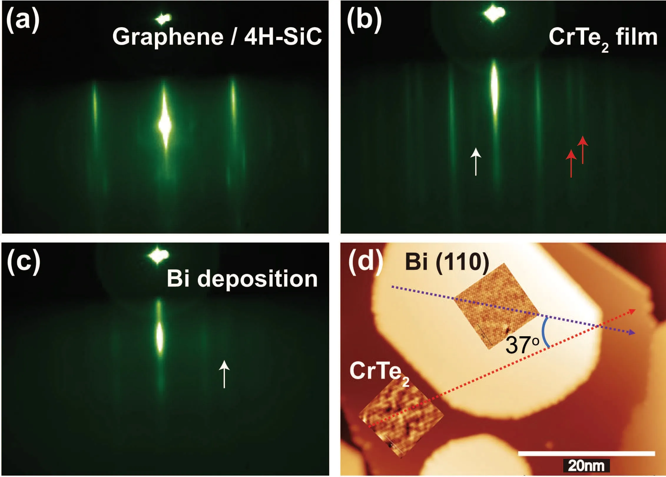
Fig.1.The RHEED diffraction patterns were obtained for (a) flat bilayer graphene on 4H-SiC substrate, (b) CrTe2 film grown on bilayer graphene.The red arrows in panel(b)indicate two orientations of CrTe2,and the white arrows indicate 2×1 reconstruction.(c)Bi deposited on CrTe2.The position indicated by the white arrow in panel(c)corresponds to the newly crystallized Bi film.(d) displays the sample morphology characterized by STM,showing an approximate 37◦angle between the Bi island lattice orientation and the CrTe2 lattice orientation.
We employed low-temperature high-resolution scanning tunneling microscopy (STM/STS) to confirm the quality of the thin films and study at the atomic scale.Figure 2(a) displays a large-scale (300 nm×300 nm) topography of bilayer graphene annealed on 4H-SiC.The sample surface exhibits a clear atomicresolved hexagonal lattice structure, depicted in Fig.2(b).Additionally, the Moir´e pattern produced by the stacked graphene is evident due to the flatness of the surface.Figure 2(c) exhibits the large-scale topography of CrTe2, indicating a flat surface with no higher layers except the second layer, indicating a layer-by-layer growth mode.The step height is approximately 62 ˚A, which is consistent with previous reports.[44]The corresponding atomic resolution image,shown in Fig.2(d), also displays a well-resolved hexagonal lattice, with a lattice constant of 3.87 ˚A, consistent with previous reports.[40,44]Figure 2(e) is a large-scale topography of Bi islands deposited on CrTe2, indicating a clean surface with large and smooth deposited Bi islands, showing a high heterostructure quality.The atomic resolution of the corresponding Bi islands, shown in Fig.2(f), shows a clear neartetragonal structure, which is the Bi(110) plane as shown in previous studies.[23,49–54]The measured lattice constants are 4.71 ˚A and 4.35 ˚A, similar to the previous report,[50]with the step height being around 750 ˚A, which is comparable to the previous report.[51,54]A lattice diagram of Bi(110) deposited on CrTe2,created using VESTA software,[55]is shown in Fig.2(g).The electronic local density of state on CrTe2and Bi(110) in the heterostructure structure is depicted in Figs.2(h) and 2(i), respectively.It shows that CrTe2displays good metallic density of states, in line with previous reports,[40,44]which indicates a similar magnetic structure in our CrTe2films The Bi(110)films exhibit good metal conduction under the effect of heterointerface, which indicates that the neighbor interaction between heterostructures is strong enough to have a significant impact.
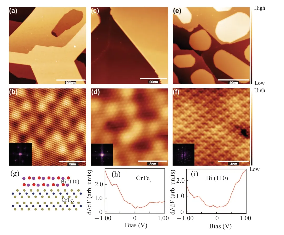
Fig.2.Atomic-scale imaging and spectroscopic characterization of the thin films.(a) Large-scale topography of bilayer graphene annealed on 4H-SiC (Vb =1 V, Iset =50 pA).(b) Atomic-resolution image of bilayer graphene showing hexagonal symmetry (inset) and Moir´e period modulation(Vb=100 mV,Iset=400 pA).(c)Large-scale topography of CrTe2 indicating a layer-by-layer growth mode(Vb=1 V,Iset=50 pA).(d)Atomicresolution image of CrTe2 showing hexagonal symmetry(inset)and a lattice constant of 3.87 ˚A.(Vb =-500 mV,Iset =500 pA).(e)Large-scale topography of Bi islands deposited on CrTe2 indicating a high-quality heterojunction (Vb =1 V, Iset =400 pA).(f) Atomic-resolution image of Bi islands showing a clear near-tetragonal structure corresponding to the Bi(110)plane with a lattice constant of 4.71 ˚A and 4.35 ˚A.(Vb=-50 mV,Iset=600 pA).(g) Model diagram of Bi(110) deposited on CrTe2.(h) and (i) Electronic localized density of state spectra on CrTe2 and Bi(110) in the heterojunction structure, respectively, indicating strong neighbor interaction between heterojunctions.
After verifying the quality of the heterostructures,we focus on exploring the interplay between the 2D magnetism of CrTe2and the topological properties of Bi(110).As shown in Fig.3, we investigated two Bi(110) islands with sizes larger than 20 nm to examine the changes in their supposed edge states with the participation of magnetic neighbors.Figure 3(a)displays the topography of a Bi(110)island on CrTe2,which forms a lateral heterostructure with CrTe2along the inplane direction due to the barrier of the boundary of the second layer of CrTe2.
In Fig.3(b),we collected the density of states of multiple points along the direction of the blue arrow in Fig.3(a)aligning with the[01¯1]direction of Bi(110).It can be observed that the density of state significantly changes at the step of Bi(110),as indicated by the yellow dotted line in the figure.The density of state at negative voltage bias exhibits an overall significant decrease at one edge (blue), while the other edge (red) does not experience such a reduction, which could be attributed to the atomic buckling effect.[54]However,unlike the previously observed edge states on Bi(110)or Bi(111),[9,10,18,21,56]we did not find any significant edge states on the step near the Fermi level in our measurements.Meanwhile, we observed an enhancement of the density of state around 350 meV at the step edge,which is distinct from the bulk state.This phenomenon is also clearly demonstrated in Figs.4(c)–4(e).We obtained results shown in Figs.3(c)and 3(d)at another Bi(110)island with the same method, which are consistent with Figs.3(a)and 3(b), demonstrating the robustness of our findings.We will comprehensively discuss these phenomena later.
Additionally, we observed intriguing yet unexplained phenomena in the measurements depicted in Fig.3.It is noteworthy that a significant enhancement in the density of states appears on the bulk states of Bi(110) at an energy of about 100 meV.This energy position aligns precisely with the energy at which the topological edge state of Bi(110)was reported in previous studies.[10,23]However,this enhancement of the density of state is not observed at the step edge.Furthermore,on the underlying CrTe2, there is also an increase in the density of state at the close energy level.Although we believe that the underlying mechanism of this phenomenon is closely related to the 2D magnetic properties of CrTe2and the topological properties of Bi(110), further investigations are necessary to clarify it.
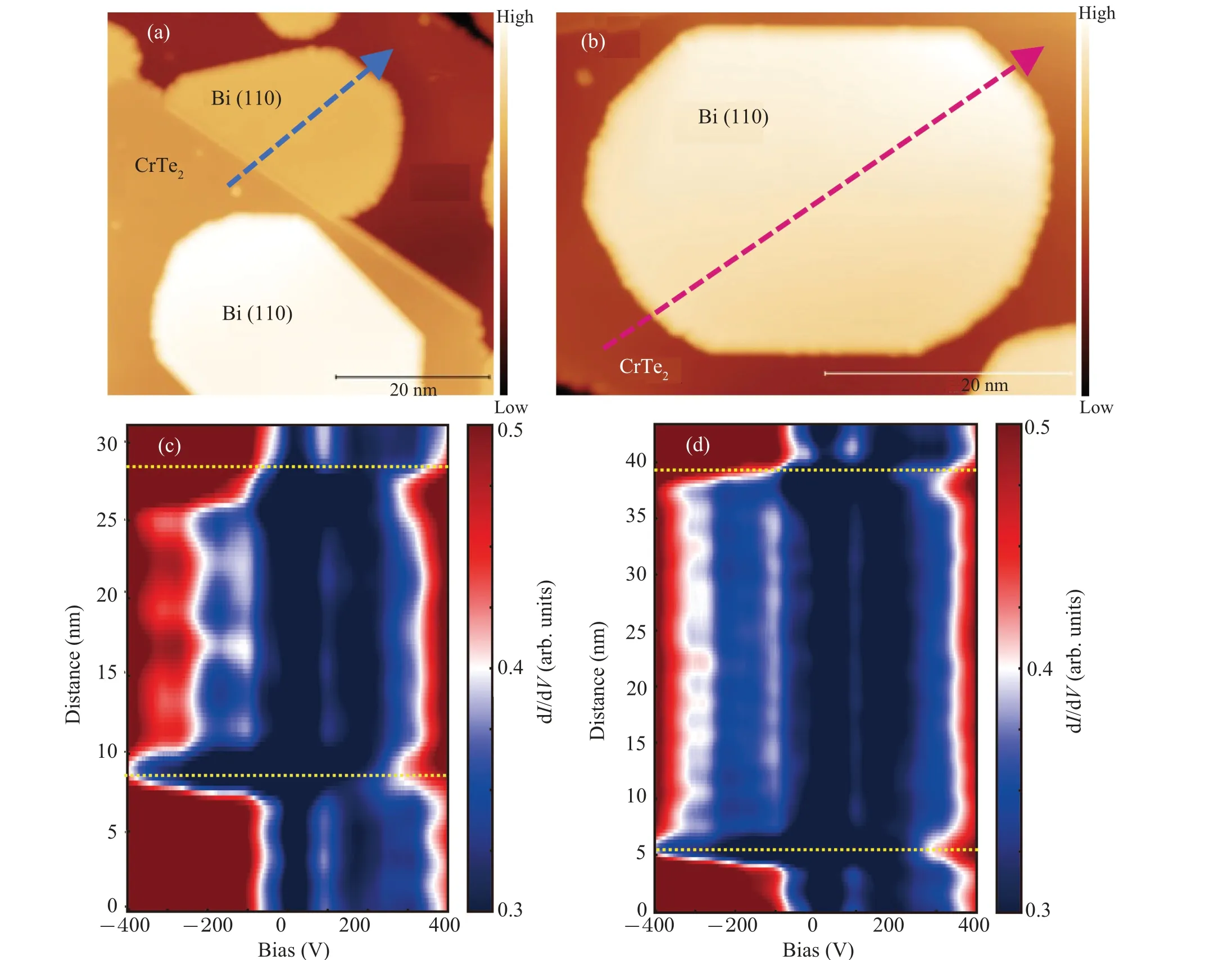
Fig.3.Exploration of the changes in the boundary state of Bi(110) on CrTe2.(a) Morphology of a Bi(110) island on CrTe2, forming a transverse heterojunction in the in-plane direction.(Vb =1 V, Iset =50 pA).(b) Density of states of multiple points along the direction of the arrow in panel (a),showing significant changes in the density of states spectrum at the step of Bi(110)(marked by the yellow dotted line),but no significant edge states were found.(c)and(d)Results consistent with panels(a)and(b),confirming the robustness of the findings.
In our few layers CrTe2case, there should be some inplane magnetism component because the in-plane nature of magnetism in monolayer CrTe2.There are some theoretical proposals[57]that if the edge state near the Fermi level of the topologically non-trivial Bi(110)is gapped due to the potential existence of an in-plane ferromagnetic component in CrTe2,it would give rise to corner states associated with highorder topological states.To investigate this possibility,we performed an detailed mapping near the boundary,as depicted in Fig.4.
Figure 4(a) displays the location and size of the Bi(110)islands selected for mapping, while figure 4(b) shows the topography of the blue box part in Fig.4(a).The sharp edges of the island prevent complex scattering effects caused by rough edges and impurities.Additionally, the use of 50 nmscale islands avoids the change in the density of states caused by finite size effects from the small area of the island.Figures 4(c)–4(h)display density of state mappings at several selected energy levels, with the corresponding color bar positioned on the right side of the figure.At higher energy levels(Figs.4(c)–4(e)),an about 2 nm-wide edge state is evident at the step edge, a phenomenon strikingly akin to the topological edge states above the Fermi level previously reported in Bi(111).[21]Hence, there is a strong possibility that this may indeed represent a nontrivial topological edge state above the Fermi level.Furthermore, our density of states mapping results did not reveale any evidence of topological corner states in Bi(110)/CrTe2films, as shown in Figs.4(c)–4(h).This indicates that the weak coupling between in-plane magnetic and topological edge states in this magnetic heterostructure.
Although theoretical predictions have suggested the possible topological edge states near the Fermi level in the Bi(110) system, our experimental findings indicate the absence of such topological edge states near the Fermi level in the Bi(110)/CrTe2magnetic heterostructure.Instead our observations suggest the potential presence of edge states similar with the topological edge states found in the Bi(111) system at a higer energy positions.In the theoretical predictions, the black phosphorus(BP)phase structure of Bi(110)was deemed crucial for the formation of topological states.This suggests that the significant lattice mismatch in the Bi(110)/CrTe2heterostructure may have an impact on the BP structure of Bi(110), which disrupts the expected topological edge states near the Fermi level.Therefore, the lattice constant of magnetic substrate is important for the high-quality Bi(110)films with the BP structure.In order to minimize the influence of buckling,substrates with a high density of state near the Fermi level should be chosen.Table 1 presents a list of experimentally verified 2D magnetic materials that could serve as potential options for magnetic substrates in constructing high-order topological magnetic heterostructures with 2D Bi.
Table 1.Experimentally confirmed typical 2D ferromagnetic materials and their lattice constants.
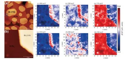
Fig.4.Detailed mapping near the boundary of Bi(110) islands.(a) Location and size of the selected islands for mapping (Vb =1 V, Iset =50 pA).(b)Morphology of the blue box part in panel(a),showing the sharp edges of the island(Vb =500 mV,Iset =500 pA).(c)–(h)Density of state mapping at selected energies,indicating the energy range in which the density of state is transferred.The color bar is consistent with that used in Fig.3.
4.Conclusions
In conclusion, we have grown a high-quality Bi(110)/CrTe2magnetic heterostructure and investigated its electronic properties along with potential topological characteristics.Our findings suggest the absence of topological edge states near the Fermi level,possibly due to the significant lattice mismatch.However, we have discovered an engaging edge state at higher energy positions on the Bi(110) surface which bears a resemblance to the topological edge state previously reported on the Bi(111) surface.[21]This could be a consequence of interplay between magnetism and topology,necessitating further theoretical investigation of this magnetic heterostructure system.To mitigate lattice mismatch and better realize the interplay between magnetism and bismuth’s topological states, we propose several alternative magnetic substrate materials that are more suitable for growing magnetic heterostructures.This study provides a foundation for future research in the fields of topological insulators, twodimensional magnetism,and heterostructure physics.
Acknowledgments
We would like to express our gratitude to Guang Bian from the University of Missouri,and to Xiaoqian Zhang from Southern University of Science and Technology for their valuable discussions and insights.
The work at IOP is supported by grants from the National Natural Science Foundation of China (Grant No. 2032204),the Ministry of Science and Technology of China (Grant No. 2022YFA1403800), and the Chinese Academy of Sciences (Grant No. XDB33000000).
- Chinese Physics B的其它文章
- Unconventional photon blockade in the two-photon Jaynes–Cummings model with two-frequency cavity drivings and atom driving
- Effective dynamics for a spin-1/2 particle constrained to a curved layer with inhomogeneous thickness
- Genuine entanglement under squeezed generalized amplitude damping channels with memory
- Quantum algorithm for minimum dominating set problem with circuit design
- Protected simultaneous quantum remote state preparation scheme by weak and reversal measurements in noisy environments
- Gray code based gradient-free optimization algorithm for parameterized quantum circuit