
Effect of surface modification on the radiation stability of diamond ohmic contacts
2024-02-29 09:17LianXiMu牟恋希ShangManZhao赵上熳PengWang王鹏XiaoLuYuan原晓芦JinLongLiu刘金龙ZhiFuZhu朱志甫LiangXianChen陈良贤JunJunWei魏俊俊XiaoPingOuYang欧阳晓平andChengMingLi李成明
Chinese Physics B 2024年2期
Lian-Xi Mu(牟恋希), Shang-Man Zhao(赵上熳), Peng Wang(王鹏), Xiao-Lu Yuan(原晓芦),Jin-Long Liu(刘金龙),†, Zhi-Fu Zhu(朱志甫), Liang-Xian Chen(陈良贤),Jun-Jun Wei(魏俊俊), Xiao-Ping Ou-Yang(欧阳晓平), and Cheng-Ming Li(李成明),‡
1Institute for Advanced Materials and Technology,University of Science and Technology Beijing,Beijing 100083,China
2School of Mechanical Engineering,University of Science and Technology Beijing,Beijing 100083,China
3School of Information Engineering,Zhengzhou University of Technology,Zhengzhou 450044,China
4State Key Laboratory of Intense Pulsed Radiation Simulation and Effect,Northwest Institute of Nuclear Technology,Xi’an 710024,China
Keywords: single crystal diamond,ohmic contact,surface modification,electron radiation
1.Introduction
Diamond has many excellent properties, such as a high breakdown field,high carrier saturation velocity and high thermal conductivity, and is an ideal choice for next-generation semiconductor devices,especially in harsh environments.Diamond field-effect transistors have shown promising performance in high-power and high-frequency operations.[1,2]Diamond radiation detectors have also been used in large-scale scientific facilities,such as the radial neutron camera and HL-2A tokamak.[3,4]In addition, as the core component of solarblind detection and imaging systems, solar-blind photodetectors have become a focus of research.Fast response to solarblind ultraviolet is also one of the important applications of diamond detectors.[5,6]
Due to the chemical inertia of diamond, it is difficult to achieve strong interface bonding and a low barrier potential between the metal electrode material and diamond simultaneously.The electrons generated by radiation, under the action of the applied electric field,will accumulate charge in the crystal and build an internal electric field if the electrical contact is not able to extract and inject electrons fast enough.Therefore, the good electrical properties of diamond are unable to be fully exploited.[7]Surface modification and a diamond-like carbon layer have been used to optimize the diamond ohmic contact.[8–10]As the common terminations of diamond, hydrogen and oxygen(H-diamond and O-diamond)have demonstrated different surface properties.For instance, H-diamond shows a negative electron affinity(NEA)and surface conductivity, but under continuous low-energy electron irradiation,the secondary electron emission intensity of H-diamonds films is decayed.[11]O-diamond can be used as an excellent surface isolation and passivation layer.In addition,radiation stability is also important for device application.Diamond detectors were irradiated by proton beams with an energy of 4.5 MeV and the results indicated that with increase in the proton fluence the charge collection efficiency was decreased.[12]Adeet al.[13]studied the radiation resistance of high-pressure/hightemperature(HPHT)and chemical vapor deposited diamonds under 6 MeV–14 MeV electron therapy beams.The results showed that HPHT diamond had better stability of response to radiation.
During the preparation of a diamond radiation detector,the performance of the device is determined by the diamond material and interface.At present, research has mainly focused on the influence of radiation on device performance and the diamond material.However, the mechanism of the influence of high-energy radiation on the diamond ohmic contact has not been systematically studied.In order to further improve the performance of diamond detectors and realize the application of diamond in electronic devices it is necessary to understand and control the influence of different terminal diamond surfaces on the contact resistance of the metal/semiconductor interface and the stability under highenergy irradiation.Due to a low contact resistance originating from an excellent affinity with carbon and relatively high diffusivity in diamond,after annealing Ti forms carbides with diamond.Heating above 425◦C caused transition from a rectifying to an ohmic contact.The ohmic property was retained during annealing at 750◦C for less than 60 min,even though Ti was diffused to the surface.[14]
In this study, H-diamond was prepared using HPHT diamond in a hydrogen plasma environment.O-diamond was obtained using HPHT diamond and heating in acid at high concentration.Based on the transmission line model (TLM),we researched the influence of surface modification technology on a diamond ohmic contact using typical electrode materials (Ti/Pt/Au) under high-energy radiation.Before radiation, the specific contact resistivities (ρc) of H-diamond and O-diamond were measured under the same conditions.After high-energy electron radiation of 10 MeV,ρcwas measured and the interface resistance between H-diamond and Odiamond was analyzed.
2.Experiment
A schematic diagram of the process for preparing diamond ohmic contacts for H-diamond and O-diamond is shown in Fig.1.Two Ib type HPHT single-crystal (100) diamonds with a size of 4 mm×4 mm were used in this experiment.The substrates were fine polished to obtain a relatively flat surface.The pressure and time were 550 Pa and 10 min,respectively, and the surface roughness was less than 1 nm.After polishing, the samples were boiled in acidic solution(HNO3:H2SO4=1:3 by volume)for 30 min and ultrasonically cleaned in acetone, alcohol and deionized water sequentially for 15 min to obtain O-diamond and remove the non-diamond impurities.The H-diamond epitaxial layer was prepared based on the O-diamond in a self-made microwave plasma chemical vapor deposition (MPCVD) system.The cavity pressure,microwave power,H2flow rate,CH4flow rate and time were 9.1 kPa,1300 W,300 sccm,0.9 sccm and 30 min,respectively.
By photolithographic technology, an area of 100 µm×100 µm with unequal spacing was patterned on H-diamond and O-diamond.Ti(10 nm)/Pt(20 nm)/Au(100 nm)were prepared by electron beam evaporation on both H-diamond and O-diamond.After the electrode was plated, the H-diamond and O-diamond were annealed at 680◦C for 30 min under hydrogen plasma to form a conductive channel and ohmic contact.The 10 MeV electron beam irradiation experiment was conducted on a linear electron accelerator.The electron flux was 3×10¹²electrons·cm-2·s-1and the irradiation time was 10 s.After irradiation, theI–Vcharacteristics of the samples were measured.
TheI–Vcharacteristics were measured with an Agilent B1500 A parameter analyzer.The quality of diamond crystal was measured by high spectral resolution analytical grade confocal Raman microscope(inVia Qontor)with a laser wavelength of 532 nm and focus spot size of 40µm.The integration time interval was 10 s,the Raman shift range was 800 cm-1–2000 cm-1, the microscopic size range was≥1 µm and the spectral resolution was 1 cm-1.A contact angle measuring instrument(DSA100)was used to characterize the wettability of H-diamond and O-diamond surfaces.
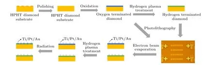
Fig.1.Schematic diagram of the process for preparing diamond ohmic contacts for H-diamond and O-diamond.
3.Result and discussion
The Raman spectroscopy characterization results using a 532 nm laser are shown in Fig.2.The Raman characteristic peaks and their full width at half maximum of H-diamond and O-diamond were 1332.53 cm-1and 1332.61 cm-1and 6.77 cm-1and 6.75 cm-1, respectively.The stress (P) in the diamond samples can be expressed asP=∆ν/k, where∆νis the displacement of the Raman characteristic peak of single-crystal diamond relative to the unstressed Raman peak andkis the Raman stress factor of diamond, which has been measured as 1.9 cm-1·GPa-1.The Raman displacement of natural synthetic diamond at room temperature is 1332.3±0.2 cm-1.[15]In this study,Pin the H-diamond and O-diamond was-0.12 GPa and-0.16 GPa,respectively.The D peak (1350 cm-1) and G peak (1580 cm-1) of the disordered carbon and graphite were not observed in the Raman spectrum.[16]
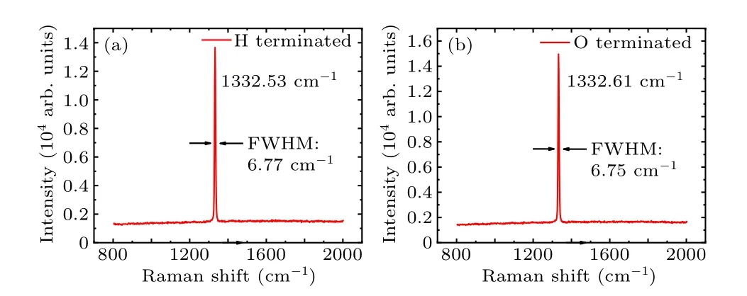
Fig.2.Laser Raman spectra of (a) H-diamond and (b) O-diamond at 532 nm excitation.
The surface properties of H-diamond and O-diamond were studied with a contact angle measuring instrument.The contact angles of deionized water on H-diamond and Odiamond were 91.5◦and 52.5◦, respectively.Wetting theory shows that for the same external adsorption medium, the smaller the surface energy of the solid surface the larger the contact angle, which shows hydrophobicity.Ostrovskayaet al.[17]obtained the surface free energies of H-diamond and O-diamond as 47 mJ·m-2and 65.8 mJ·m-2, respectively.O-diamond was achieved by introducing oxygen-containing functional groups such as C–O, C=O and –COOH, on the surface.[18]H-diamond was prepared under hydrogen plasma treatment after heating with strong oxidizing acids.The corresponding dangling bonds are occupied by hydrogen atoms or hydrogen molecules.The hydrocarbon groups induced by the hydrogen plasma treatment reduce the surface free energy and lead to hydrophobicity of the diamond surface.The surface area of H-diamond mainly comprises hydrogen functional groups such as C–H.[19]The main reason for the large difference between the contact angles of H-diamond O-diamond is that the different surface adsorption groups cause surface reconstruction,giving different surface free energies.
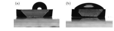
Fig.3.Contact angle test: (a)H-diamond and(b)O-diamond.
After annealing at 680◦C, theI–Vcharacteristic curves of H-diamond and O-diamond were measured.Ohmic contacts were formed with different spaces.The spaces designed in the photolithographic mask were 2µm,4µm,6µm,8µm and 10 µm, and the rectangle size was 100 µm2after metal plating due to accurate photolithography.For H-diamond,the spaces between adjacent rectangles were remeasured under the optical microscope as 3.8 µm, 5.3 µm, 7.0 µm, 9.1 µm and 11.4 µm, respectively, and the rectangle size was 100 µm2.The spaces between adjacent rectangles of O-diamond were 10.6 µm, 12.4 µm, 14.8 µm and 15.7 µm, respectively, and the rectangle size was 100 µm2.For TLM measurement, the total resistanceRtot(obtained fromV/I)for a rectangular geometry can be expressed as[20,21]
whereRcdenotes the total contact resistance,Rsis the semiconductor thin layer resistance between ohmic contacts,lis the space between rectangles,Wis the width of the contact pad andρcis specific contact resistivity.WhenRtotis plotted as a linear function ofl,ρccan be calculated according to Eq.(2).In Figs.4(a) and 4(c), theI–Vmeasurements are exhibited as functions of the space between two adjacent pads of the TLM pattern.It can be clearly seen that both H-diamond and O-diamond contacts have a linearI–Vcharacteristic and theRtotbetween any two adjacent contact pads can be deduced.Rtotbetween the pairs of contacts versus the contact spacinglfor H-diamond and O-diamond annealed at 680◦C is shown in Figs.4(b) and 4(d), and theρcvalues are calculated to be 2.0×10⁻⁴Ω·cm2and 4.3×10⁻³Ω·cm2,respectively,according to Eq.(2).Theρcvalue is comparable to Chen’s report,[22]in which the specificρcvalue of boron-doped diamond and a Ti/Pt/Au metal electrode was 10-4Ω·cm2.

Fig.4.TLM I–V characteristics of (a) H-diamond and (c) O-diamond with different spacings between two adjacent patterns, before radiation.Dependence of Rtot on l for(b)H-diamond and(d)O-diamond.
In order to test the stability of H-diamond and Odiamond,10 MeV electron beam irradiation experiments were carried out in a linear electron accelerator.The electron flux was 3×10¹²electrons·cm-2·s-1and the irradiation time was 10 s.After irradiation, theI–Vcharacteristic curves of the samples were tested.As shown in Figs.5(a)and 5(c),theI–Vcharacteristic curves of H-diamond and O-diamond are linear,forming an ohmic contact.As shown in Figs.5(b)and 5(d),by calculation theρcvalues for H-diamond and O-diamond after radiation are 5.3×10⁻³Ω·cm2and 9.1×10⁻³Ω·cm2,respectively.Figure 6 summarizes the change inρcof H-diamond and O-diamond before and after irradiation.

Fig.5.TLM I–V characteristics of (a) H-diamond and (c) O-diamond with different spacing between two adjacent patterns,after radiation.Dependence of Rtot on l for(b)H-diamond and(d)O-diamond.
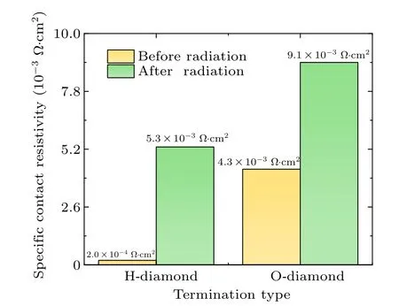
Fig.6.Specific contact resistivity before and after irradiation of Hdiamond and O-diamond.
A schematic diagram of the diamond interface before and after irradiation is shown in Fig.7.Exposure of the surface of H-diamond to air leads to the generation of surface conductance.The surface conductive channel of H-diamond is located at 10 nm–30 nm below the surface,exhibiting conductivity characteristics similar to a two-dimensional hole gas.[23,24]This model suggests that the adsorption of materials with low unoccupied electron states on the surface of H-diamond is a sufficient condition for surface conductivity.In order to accumulate enough holes in the subsurface region of the diamond when hydrogen acts as an impurity level, valence band electrons can be realized by transiting to the adsorption layer of the low unoccupied energy state, and a doping effect is achieved by electron transfer.[25]Therefore, H-diamond shows p-type conductivity and has a NEA.The work function of the surface of H-diamond exposed to air is about 5.3 eV.[26]The electron affinity of(100) H-diamond is-1.3 eV to-0.4 eV.[27,28]Odiamond has a positron affinity of 1.7 eV.[29]Zhanget al.[30]demonstrated that O-diamond can efficiently pin the Fermi level in a fixed position regardless of the metallic material.Because H-diamond has NEA it is conducive to electron transmission when forming an ohmic contact.TheI–Vcurve measurement results show thatRtotandρcof H-diamond are lower than those of O-diamond.H-diamond can reduce the resistance and improve ohmic contact.After 10 MeV electron radiation,Rtotandρcof H-diamond and O-diamond increased.The rates of change ofρcof H-diamond and O-diamond after radiation were 2550%and 112%,respectively.The reason for the increase in contact resistance is explained below.Generally,an O-termination is more stable than an H-termination on the diamond surface.Foordet al.[31]observed that the uptake of oxygen on O-diamond was slower than on H-diamond,and an explanation for the enhanced reactivity could be that the hydrogenation used here essentially roughened the surface,thus leading to more surface sites on which oxygen could adsorb.For the H-terminated diamond, 10 MeV electron radiation would promote the formation of C=O bonds, reducing the number of C–H bonds on the surface.[32]Meanwhile,electron beam bombardment destroys the H-diamond and decreases the film’s NEA, resulting in substantial degradation of surface conductivity.[33]After irradiation, the C=O bonds were enhanced, which is the main reason for the increase in contact resistance of O-terminated diamond.[32]The increase in interface resistance caused by radiation may also be an important factor leading to degradation of the performance of diamond detectors.
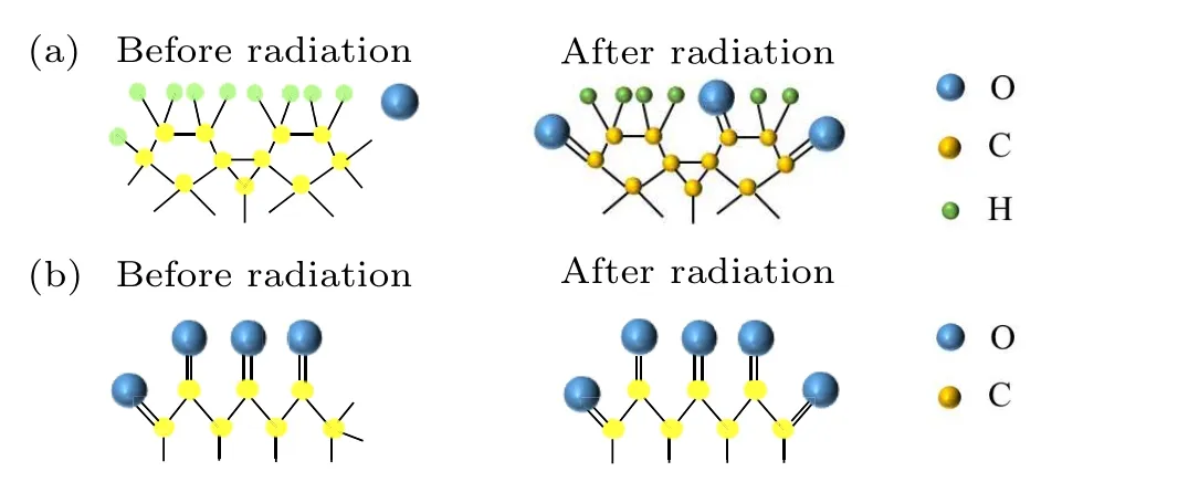
Fig.7.Schematic diagram of the diamond interface before and after radiation: (a)H-diamond and(b)O-diamond.
4.Conclusion
In this work,based on the TLM,the influence of surface modification technology on diamond ohmic contacts was researched.After annealing, the specific contact resistivities of H-terminated diamond–Ti/Pt/Au and O-terminated diamond–Ti/Pt/Au were 2.0×10⁻⁴Ω· cm2and 4.3×10⁻³Ω·cm2, respectively.After 10 MeV electron radiation,the specific contact resistivities of H-terminated diamond and O-terminated diamond were 5.3×10⁻³Ω·cm2and 9.1×10⁻³Ω·cm2, respectively.After radiation,the rates of change of specific contact resistivity of H-terminated diamond and O-terminated diamond were 2550% and 112%, respectively.By contrast, Hterminated diamond showed lower resistivity, while the surface of O-terminated diamond was relatively stable.
Acknowledgment
Project supported by the National Key Research and Development Program of China(Grant No.2022YFB3608601).
猜你喜欢
华人时刊(2023年19期)2023-11-16
Chinese Physics B(2023年9期)2023-10-11
Chinese Physics B(2023年7期)2023-09-05
中等数学(2022年9期)2022-11-17
北方音乐(2018年17期)2018-10-31
小哥白尼(野生动物)(2018年4期)2018-08-01
电影文学(2017年2期)2017-12-26
棋艺(2016年4期)2016-09-20
水动力学研究与进展 B辑(2015年2期)2015-04-20
- Chinese Physics B的其它文章
- Unconventional photon blockade in the two-photon Jaynes–Cummings model with two-frequency cavity drivings and atom driving
- Effective dynamics for a spin-1/2 particle constrained to a curved layer with inhomogeneous thickness
- Genuine entanglement under squeezed generalized amplitude damping channels with memory
- Quantum algorithm for minimum dominating set problem with circuit design
- Protected simultaneous quantum remote state preparation scheme by weak and reversal measurements in noisy environments
- Gray code based gradient-free optimization algorithm for parameterized quantum circuit