
A flexible ultra-broadband multi-layered absorber working at 2 GHz–40 GHz printed by resistive ink
2024-02-29 09:17TaoWang汪涛YuLunYan闫玉伦GongHuaChen陈巩华YingLi李迎JunHu胡俊andJianBoMao毛剑波
Chinese Physics B 2024年2期
关键词:汪涛
Tao Wang(汪涛), Yu-Lun Yan(闫玉伦), Gong-Hua Chen(陈巩华), Ying Li(李迎),Jun Hu(胡俊), and Jian-Bo Mao(毛剑波)
1School of Microelectronics,Hefei University of Technology,Hefei 230601,China
2Special Display and Imaging Technology Innovation Center of Anhui Province,Academy of Photoelectric Technology,Hefei University of Technology,Hefei 230027,China
Keywords: extra broadband,physical model,flexible metamaterial absorber,multi-layer,frequency selective surface
1.Introduction
To date,frequency selective surface(FSS)microwave absorbers have been studied extensively because of their potential applications in electromagnetism stealth and electromagnetic compatibility.Usually, an FSS microwave absorber is required to work at extra broad bandwidth with low reflectivity and minimal thickness, but it is hard to implement.[1]When a plane microwave is incident on the surface of an FSS absorber,the impedance of the air and the absorber should be perfectly matched to reduce reflection.Due to the fact that the absorption bandwidth of metamaterial is limited, bandwidthenhanced absorbers were developed by combining two distinct resonators together,and stacked layer by layer.[2,3]
To date, circuit analogue absorbers (CAs) with periodic arrangement cells have been explored to further expand the bandwidth of the FSS absorber; this is usually composed of a conductive pattern and a lossy element,printed on a dielectric substrate and supported by a metal plate.Lossy components play a major role in an FSS absorber, and resistors,[4,5]resistive ink structures,[6–8]or resistive thin films are three of the most important lossy components.[9]Windmill-shaped elements were used in a broadband metamaterial absorber with measured absorption over 90%at 8.3 GHz–17.4 GHz.[10]Resistive films were adopted in a broadband absorber, and the absorptivity exceeded 90%at 6.06 GHz–14.66 GHz.[11]Shuiet al.reported a flexible and thin Ti3C2TXsponge composite absorber working at 0.3 THz–1.65 THz with absorption over 90%and with a thickness of about 2 mm.[12]The above literature suggested that both materials and structures can be explored to improve the absorption performance,[13–18]and thus the absorption bandwidth can be expanded with relatively minimal thickness.
Based on the works mentioned above, a flexible multilayer ultra-broadband absorber stacked with five layers is modeled in this work;each layer is separated by a PVC spacer and is printed with resistant ink patterns.According to the physical model and the electric circuit model,the reflectance is less than-10 dB at 1.998 GHz–40.056 GHz, and the fractional bandwidth(FBW)is 181.1%with a thickness of 0.098λmaxat the maximum wavelength of the absorption band.Additionally, this absorber is fabricated and verified, and the experimental results are very consistent with the simulation.
2.Physical model and electric circuit model of the flexible absorber
The multi-layer broadband absorber is composed of five lossy layers and a metal plate.Each layer is a PI(ε=3.24+j0.031)substrate printed with resistive ink patterns on the upper surface.The upper and lower layers are separated by PVC(ε=2.56+j0.025) dielectric material.A metal plate at the bottom of the absorber,which acts as a ground layer,is used to eliminate transmission.The unit cell geometry of this absorber is depicted in Fig.1(a).The geometrical dimensions are as follows:P=13 mm,l1=12 mm,l2=11.4 mm,l3=6.8 mm,l4=10.8 mm,l5=7 mm,h1=h2=h3=h4=h5=2 mm,h6=4 mm,h7=0.15 mm.The thickness of the resistive ink patterns is about 0.05 mm, with conductivity of 120 Ω/sq.Since PI acts as a transmission line, an equivalent circuit of the absorber can be modeled as parallel connections between transmission lines and series RLC circuits,as shown in Fig.1(b).
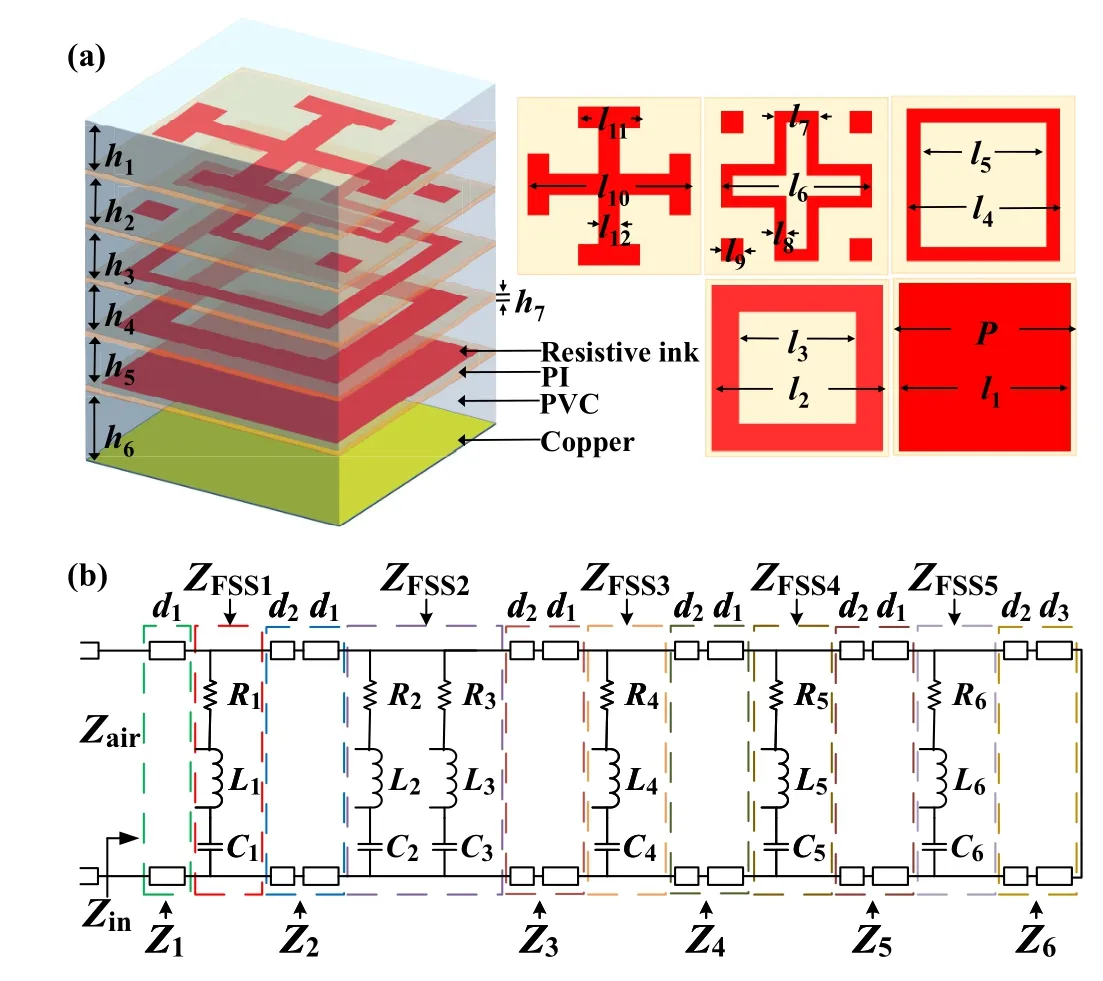
Fig.1.(a)The physical model of the flexible absorber,(b)the equivalent circuit of the physical model.
A three-dimensional fullwave finite element method simulation of the physical model is developed in Microwave Studio software with periodic boundary conditions,which is compared with an equivalent circuit method using software, as shown in Fig.2.The reflectance of this absorber is less than-10 dB across S, C, X, Ku, K and Ka bands at 1.998 GHz–40.056 GHz, which provides a relative bandwidth of 181.1%with a total thickness of 0.098λmaxat the lowest frequency.
Both the minimum reflection and the perfect absorption can be obtained if the impedance of the absorber and air are perfectly matched.[13]To better understand the extra-broadband mechanism of this absorber, the normalized impedance is determined.Moreover, the real part fluctuates close to 1 and the imaginary part swings near to 0 at 1.998 GHz–40.056 GHz, as demonstrated in Fig.3(a).It can be seen that the equivalent impedance of two absorption peaks is 1.00456-j0.00161 at 22.005 GHz and 1.00118-j0.01754 at 37 GHz;therefore,perfect impedance matching is achieved.Complex permittivity and permeability are calculated, which prove the strictly mono-negative characteristics of this absorber, as shown in Fig.3(b).Due to perfect impedance matching, the resonance absorption is less than-40 dB at 22.005 GHz and-30 dB at 37 GHz; therefore, the incident wave is absorbed completely at 22.005 GHz and 37 GHz.In addition,due to the fact that the maximum deviation between the effective impedance and 1+j0 is less than 0.16 at 2 GHz–40 GHz,the absorptivity is more than 90%at 2 GHz–40 GHz.However,the perfect impedance matching of the suggested absorber is mainly caused by the multi-layer structure and electromagnetic characteristics of the materials.
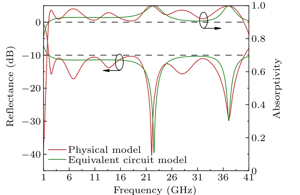
Fig.2.A comparison of the physical model analysis and equivalent circuit analysis.
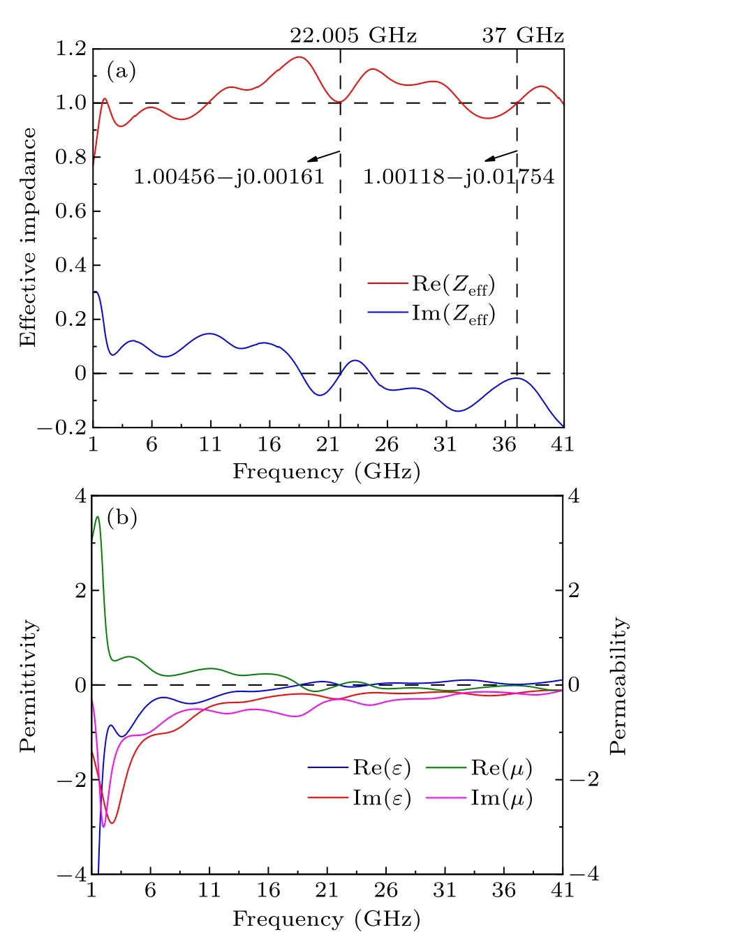
Fig.3.Characteristics of the absorber: (a)effective impedance,(b)complex permittivity and permeability.

Fig.4.The MFD and SCD on each layer:(a1)–(f1)MFD at 22.005 GHz,(a2)–(f2)SCD at 22.005 GHz,(a3)–(f3)MFD at 37 GHz,(a4)–(f4)SCD at 37 GHz.
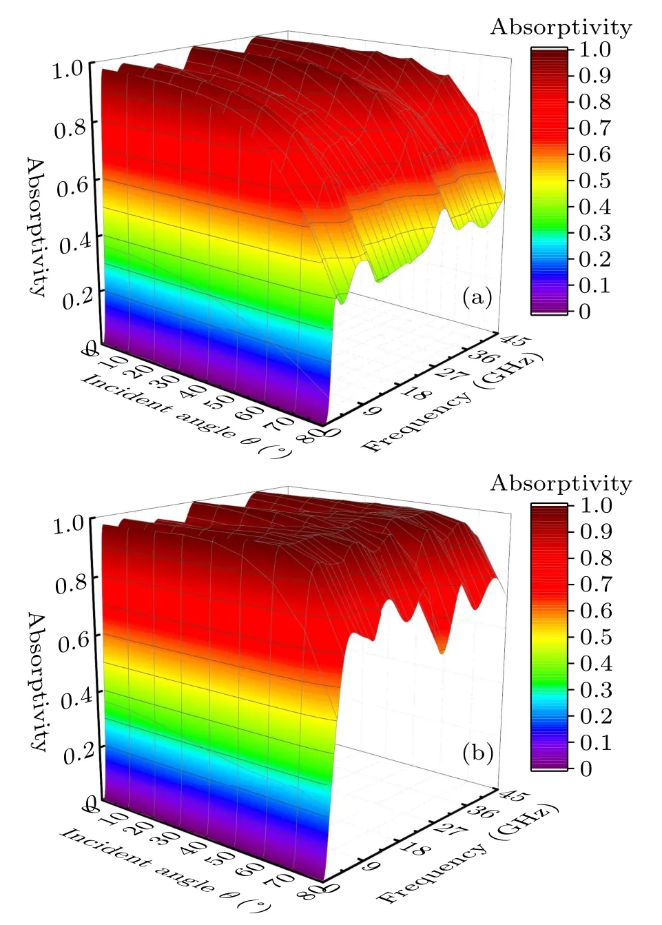
Fig.5.The absorption spectrum of the plane wave versus the incident angle: (a)TE wave,(b)TM wave.
Impedance matching between metamaterials and air plays a crucial role in electromagnetic resonant characteristics, and will enlarge the absorption bandwidth.According to Fourier transform, all incident plane waves are composed of sine or cosine waves with independent resonant frequencies.Furthermore, resonant structures composed of inductors and capacitors in the metamaterial will generate several LC resonances.In general,the resonant characteristics of the device structure will lead to absorption characteristics of the device in the resonance frequency band.Based on the superposition principle,if each LC resonant structure in the metamaterial absorbs electromagnetic waves independently,then the combination of multiple LC resonant structures will obviously increase the absorption bandwidth.
To further investigate the extra broadband wave absorption mechanism of this multi-layer absorber,the magnetic field distribution(MFD)and surface current distribution(SCD)on each layer at two absorption peaks, i.e., 22.005 GHz and 37 GHz, are simulated using near-field conditions.The intensity and density of the MFD and SCD at 22.005 GHz are shown in Figs.4(a) and 4(b).It can easily be seen that the current direction on FSS1and FSS5is opposite to that on the ground; therefore, a loop is generated, which leads to strong magnetic resonance and storage of electromagnetic energy.Moreover,another strong magnetic resonance is generated between the FSS3layer and FSS5layer due to the opposite current.As a result, the energy of the incident electromagnetic wave is absorbed and transformed to magnetic energy, which is mainly stored on the FSS3layer and on the FSS5layer.The intensity and density of the MFD and SCD at 37 GHz are shown in Figs.4(c) and 4(d).The energy of the incident electromagnetic wave is absorbed and stored on each layer discretely; the energy is mainly stored in the center of the FSS1layer and the corners of the FSS3layer.
Simulation of the absorptivity at various incident angles(θ) for both transverse electric (TE) and transverse magnetic(TM) polarization plane waves are shown in Fig.5.As can be observed,the absorption is insensitive to the change in polarization angles,but the absorption and bandwidth are dependent on the incident angle(θ);the absorption rates of both TE waves and TM waves exceed 80% whenθis less than 50◦.For the TE wave, the absorption is abruptly dropped whenθexceeds 70◦.In comparison,the absorptivity is more than 0.6 whenθis equal to 80◦for the TM incident wave.
3.Fabrication and measurement verification
To verify the actual characteristics of the above discussed absorber,an absorber is fabricated based on Fig.1(a)for measurement.Each resistive pattern is printed on a PI sheet using resistive ink,with resistance of 120 Ω/sq and with a thickness of 0.050 mm.Here, 20×20 cells are contained in the fabricated absorber, with a total size of 270 mm×270 mm and with a total thickness of 14.75 mm; the measurement of the sample is shown in Figs.6(a) and 6(b).In the experiment,two horn antennas, acting as a transmitting end and a receiving end,are connected to a vector network analyzer(Rohde&Schwarz,ZVA40),and the position of the fabricated absorber is adjusted to remain perpendicular to the axis of the horn antennas,as shown in Fig.6(c).
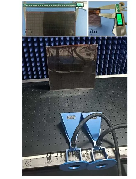
Fig.6.Measurement of the fabricated absorber sample:(a)size,(b)thickness,(c)the measurement system in a microwave anechoic chamber.
TheS-parameter of the fabricated absorber can only be measured at 8 GHz–40 GHz, due to the lack of horn antennas working at 2 GHz–8 GHz.However, a few burrs in the measurement may be caused by environmental noise,temperature noise and higher harmonics that are inevitably produced because of the test cables between the horn antenna and the vector network analyzer.Deviations between the experiment and simulation in the frequency spectrum may be caused by near-field coupling effects between the upper resistive ink patterns and the bottom metal plane,the mutual coupling between array cells and the limited size of the proposed metamaterial sample,and calibration of the transmission line system in the microwave anechoic chamber, which was used for measurement,as shown in Fig.7(a).
To verify the flexibility of the absorber, the fabricated absorber conforms to the external surface of a cylinder withD=200 mm andD=100 mm, respectively.The normalized absorption spectrum is shown in Fig.7(b), which shows good flexibility of the fabricated absorber since the measured absorption rates are all above 80%.

Fig.7.(a)The measured absorptivity vs.simulation,(b)the comparison of the plane and the curved absorbers.
A comparison of this MMA with other recently reported microwave absorbers is shown in Table 1, whereλmaxis the maximum wavelength in the absorption spectrum.The key parameters of the MMA, such as the absorption bandwidth,relative bandwidth,periodicity and thickness are listed here.It should be pointed out that the structure and performance of this absorber are quite different from those from
Refs.[13–17].This is due to the fact that this absorber is fabricated using excellent flexible materials and the fact that it shows ultra-wideband microwave absorption capability,i.e.,it covers whole S,C,X,Ku,K,Ka bands,and parts of L and U bands.
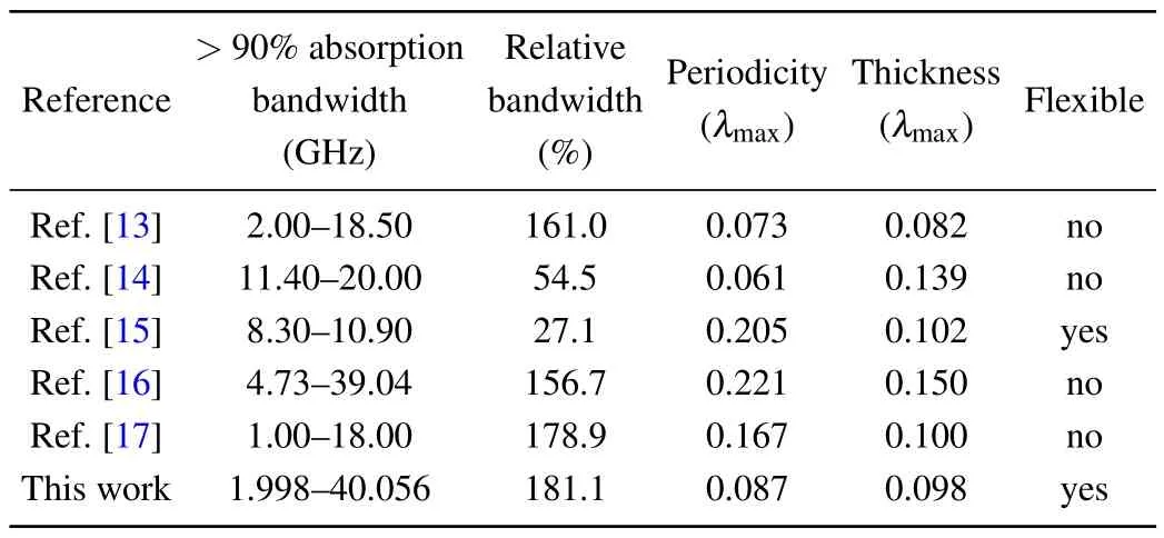
Table 1.A comparison of the suggested absorber with typically reportedabsorbers.
4.Conclusion
A flexible five-layer extra-broadband absorber printed by resistive ink on dielectric sheets and separated by PVC is discussed.An equivalent circuit model is built to explain the impedance matching mechanism of this absorber.In addition,three-dimensional full wave analysis is used to study the electric current distribution and magnetic field distribution of each layer.For verification,the absorber is fabricated and measured in a microwave anechoic chamber;both the simulation and experimental results reveal good absorption performance from 1.998 GHz to 40.056 GHz.Compared with broadband absorbers reported recently, it can be noted that the biggest relative bandwidth ratio and the smallest thickness are realized in this work, which illustrates its potential electromagnetism applicability in stealth and compatibility.
Acknowledgments
Project supported by the China Post-doctoral Science Foundation (Grant No.2020M671834) and the Anhui Province Post-doctoral Science Foundation,China(Grant No.2020A397).
猜你喜欢
——记重庆市永川监狱民警汪涛
当代党员(2022年13期)2022-07-25
物流科技(2022年2期)2022-05-07
Chinese Physics B(2022年3期)2022-03-12
Chinese Physics B(2022年1期)2022-01-23
房地产导刊(2021年11期)2021-11-27
房地产导刊(2021年10期)2021-11-22
中学生数理化·高三版(2021年10期)2021-11-01
房地产导刊(2020年6期)2020-07-25
民间故事选刊·上(2020年5期)2020-05-14
方圆(2020年23期)2020-01-07

- Chinese Physics B的其它文章
- Unconventional photon blockade in the two-photon Jaynes–Cummings model with two-frequency cavity drivings and atom driving
- Effective dynamics for a spin-1/2 particle constrained to a curved layer with inhomogeneous thickness
- Genuine entanglement under squeezed generalized amplitude damping channels with memory
- Quantum algorithm for minimum dominating set problem with circuit design
- Protected simultaneous quantum remote state preparation scheme by weak and reversal measurements in noisy environments
- Gray code based gradient-free optimization algorithm for parameterized quantum circuit