
Wideband low-scattering metasurface with an in-band reconfigurable transparent window
2024-02-29 09:17YingZhu朱瑛WeixuYang杨维旭KunDuan段坤TianJiang姜田JunmingZhao赵俊明KeChen陈克andYijunFeng冯一军
Chinese Physics B 2024年2期
关键词:杨维
Ying Zhu(朱瑛), Weixu Yang(杨维旭), Kun Duan(段坤), Tian Jiang(姜田),Junming Zhao(赵俊明), Ke Chen(陈克), and Yijun Feng(冯一军)
School of Electronic Science and Engineering,Nanjing University,Nanjing 210023,China
Keywords: metasurface,reconfigurable transparent window,radar cross section(RCS)reduction
1.Introduction
Radar cross section(RCS)is the primary indicator to assess the scattering properties of a subject.With the growing demands of stealth technologies, numerous methods, such as shaping to adjust the direction of reflected waves[1–3]or loading radar absorbing materials (RAM) to absorb the incident electromagnetic energy,[4–6]have been reported to achieve RCS reduction.Recently, metamaterials and metasurfaces,which are composed of subwavelength-scale structures, have received considerable attention and offered a new platform for engineering the target’s RCS,due to their low thickness,light weight, and designable properties.By designing meta-atoms with various shapes,rotation orientations,and spatial distributions,it is possible to tailor the amplitude,phase,polarization,and other characteristics of electromagnetic(EM)waves.[7–12]Consequently, a series of novel electromagnetic functions have been realized,such as metalens,[13–15]cloak,[16–19]holographic imaging,[20–22]etc.To achieve RCS reduction, one approach is to design a metamaterial absorber that dissipates the electromagnetic energy of incidence and converts it into ohmic loss.[23–27]For example, Ref.[27] proposes a doublelayer metasurface that consists of square patches loaded with resistors to absorb the incident waves, demonstrating that at least 10 dB RCS reduction of the antenna can be obtained from 6 GHz to 14.5 GHz.On the other hand, phase-only metasurfaces can realize low-scattering properties based on the theory of phase cancellation stemming from the specific spatial arrangement of meta-atoms.For instance, a wideband 10 dB RCS reduction can be accomplished by arranging two basic elements with 180◦±37◦phase difference into checkerboard or aperiodic configurations.Such phase differences can be attained by modifying the co-polarized reflection phase[28–30]or employing the polarization conversion metasurfaces (PCMs)that convert incidence into cross-polarized reflection.[31–33]In more recent attempts,absorption and diffusion have even been integrated into a single metasurface to effectively expand the bandwidth of RCS reduction.[34]
As one of the essential components of a radar system that protects the antennas physically, the metasurface should be transparent in the operation bands while absorbing or scattering detected waves outside the passband, making it a key component in RCS reduction.In order to design a metasurface and simultaneously ensure the radiation performance of the antenna, one attempt is putting the low-scattering frequency band outside the radiation band.[27]Another approach,known as frequency selective radome (FSR), is to include a transmission window within the wide RCS reduction band.When the bandpass frequency selective surface(FSS)layer is combined with an absorption layer or diffusion layer,the incidence can penetrate through FSR in the pass band while being consumed[35,36]or scattered[37–40]in the side bands,realizing an out-of-band RCS reduction without compromising the inband transmission performance.Nevertheless, the existence of a transmission window will allow the in-band detection signals to easily pass through the FSR and subsequently detect the antenna in practice.
Here,we propose a wideband low-scattering metasurface with an in-band reconfigurable transparent window using electrically driven PIN diodes.The operating state of the transmission window can be switched to the low-scattering state to reduce the in-band RCS by manipulating the external bias voltages of the diodes.Both simulated and measured results demonstrate that the proposed metasurface merits low profile,polarization insensitivity, low insertion loss, and wide bandwidth in both states.Additionally,since the low RCS property is accomplished by diffusion rather than absorption, the proposed metasurface does not require any resistive sheets,which reduces the complexity of circuit design and the cost of processing.
2.Design of the proposed metasurface
As schematically depicted in Fig.1, the proposed metasurface achieves obviously minimal backscattering with an in-band reconfigurable transparent window.The whole metasurface is composed of three dielectric layers separated by two air spacers.The upper and bottom layers consist of a series of orthogonal PCM elements arranged in a checkerboard pattern, while the middle layer is a switchable FSS loaded with electrically driven PIN diodes.The reconfigurable inband wave functions can be dynamically switched between beam-splitting scattering and in-band high transmission by applying different biasing voltages to the diodes.When PIN diodes work in the on state,the FSS will act as a metal ground to block the transmission of in-band incidence.As a result,the whole structure can be viewed as a checkerboard reflecting screen and the reflected wave will be split into a four-beam scattering pattern, of which the energy in the normal direction is canceled by the phase destructive interference,thus the in-band backward monostatic RCS can be significantly suppressed.On the contrary, when PIN diodes operate in the off state, the middle layer works as a bandpass FSS and the inband incident wave can penetrate through the metasurface with a negligible inset loss.For the out-of-band incident EM wave,the FSS layer always acts as a metallic ground regardless of the biasing state of the PIN diodes, so the incident energy is scattered towards the directions of four split beams,leading to the out-of-band RCS reduction.
The critical step in realizing the reconfigurable transmission window is to design a switchable FSS as the transmissionreflection control layer,of which the unit cell has a multi-layer configuration of two identical but orthotropic metallic patterns separated by a lossy substrate Rogers RO4350B (εr=3.66,tanδ=0.0037) with a thickness of 0.5 mm.Figure 2(a) depicts the pattern of the metallic layer,which consists of a cruciform patch and two parallel strips connected by two PIN diodes in the same direction.It is worth noting that the parallel strips not only contribute to the resonance of bandpass FSS, but also act as the positive and negative electrodes to provide direct current(DC)bias voltages.We can switch the two PIN diodes’ states on the same layer of the unit cell simultaneously by controlling the voltages ofV1andV2.To realize polarization insensitivity, a conventional method is to adopt a single-layer metallic configuration with a patch and a square ring, which would necessitate additional feeding lines and introduce undesired distractions in response to the incident field.In our attempts, the bottom layer is in-plane rotated by an angle of 90◦twisted to the upper layer, not only increasing the symmetry of the structure but also eliminating the EM interference from additional feeding lines.Moreover,the advantage of polarization-insensitive transmission characteristics can be achieved,due to the same electromagnetic responses between the top(bottom)layer for thex-polarized incidences and the bottom (top) layer for they-polarized incidences.Commercial PIN diodes (SMP1320-079LF) are selected as the active components, which can be modeled as a series circuit ofCOFF=0.24 pF,LOFF=0.5 nH in the off state, and as a series circuit ofRON=0.5 Ω,LON=0.75 nH in the on state.According to the equivalent parameters,when the diodes operate in the off state, a low transmission can be obtained between the two ports, which allows for the metallic patterns of the FSS structure to be separated from each other.On the contrary,when the diodes operate in the on state,high transmission can be obtained, thus the metallic patterns of FSS will be connected by the diodes, and act as a metallic ground to reflect incident waves.The other optimized geometric parameters of the element arep=16 mm,w1=1.8 mm,w2=2.3 mm,l2=11 mm,w3=4 mm,andl3=7 mm.Fullwave simulations are performed with CST Microwave Studio,where periodic boundary condition is used in bothx- andydirections to mimic the infinite periodic structure while open boundary condition is applied forz-direction.The simulated resultsS-parameters with different biasing voltages are illustrated in Fig.2(d).When the portsV1andV2are both unbiased,the PIN diodes are switched off and an equivalent capacitance will be introduced into the structure, producing a parallel LC circuit resonance that allows for the majority of incident EM energy to pass through the proposed FSS.As a result,a transmission passband is observed at 4 GHz with an insertion loss of about 0.2 dB.On the contrary, all diodes are switched on whenV1is biased to greater than twice the diode’s threshold voltage andV2is set in an unbiased state.In this case, the unit cell functions as a dual-polarized reflector with a reflection coefficient greater than-1 dB at most frequencies, thus the transmission amplitude is suppressed to about-20 dB at 4 GHz.Therefore, under forward-biased voltage, the structure exhibits high reflection and low transmission within the frequency band of a switchable transparent window.
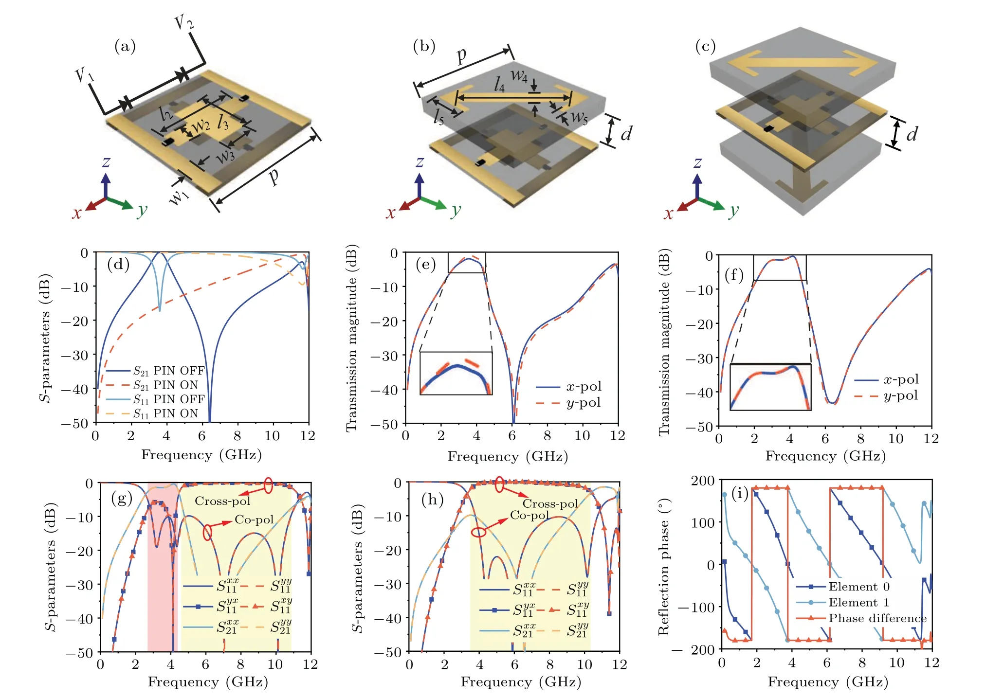
Fig.2.Schematic of unit cells for(a)the switchable FSS,(b)the metasurface with single-layer PCM,and(c)the proposed metasurface with double-layer PCM.(d)Simulated S-parameters of the switchable FSS in different states.Simulated transmission coefficients of the metasurface with(e)single-layer PCM and(f)double-layer PCM with diodes switched off.Simulated S-parameters of the proposed metasurface with diodes(g)switched off and(h)switched on.(i)Simulated cross-polarized reflection phase of the element 0 and element 1 and their phase difference when the diodes switched to the on state.
As shown in Fig.2(b),we then place a dual-arrow-shaped PCM structure over the switchable FSS with an air gap to create an element that can easily realize the 180◦reflection phase difference.The out-of-phase response of the cross-polarized reflection can be achieved through in-plane rotation of the top PCM structure by 90◦about thez-axis, without altering the bottom switchable FSS.The substrate of the PCM is selected as F4B (εr=2.2, tanδ=0.002) with a thickness of 2 mm.The optimized geometry parameters of the element are as follows:d=5 mm,w4=2.3 mm,l4=16 mm,w5=0.85 mm,andl5= 5 mm.The simulated transmission performance without biasing voltages is illustrated in Fig.2(e).Because the PCM unit cell does not entirely transmit electromagnetic waves around 4 GHz, the transmission performance of the metasurface only realizes the lowest insertion loss larger than 2 dB forx-polarized incidence.Additionally,due to the asymmetry of the structure, a slight difference is observed in the EM responses for two polarizations of incidences.
To solve the aforementioned problem, as shown in Fig.2(c), we place two orthogonal PCM layers at the same distance on both sides of the middle FSS layer, each with opposite-side metallic pattern printing.The whole unit cell functions as a Fabry–Perot-like resonance cavity, thus the transmission characteristics can be significantly improved.When the incidence illuminates the metasurface, most of the energy will first pass through the whole structure,whereas the other left will be reflected constantly between two PCM layers and finally transmit as well.When the resonator’s height or the distance between the two layers of PCM,satisfies the resonant condition, the transmitted wave can be in-phase superposed thus improving the transmission efficiency,[41]as presented in Fig.2(f).The performances of the final unit cell are then numerically calculated by employing CST Microwave Studio.When the PIN diodes are switched off,as depicted in Fig.2(g),where the red and yellow backgrounds represent the transmission band and the polarization conversion band, respectively,the operating band with co-reflection coefficient(Sxx11,Syy11)less than-10 dB ranges from 2.9 GHz to 10.85 GHz.Here, the first (second) superscript denotes the output (input) polarization and the first(second)subscript denotes the receive(transmit)port,with 1 for reflection region and 2 for transmission region.The element works in transmission mode around 4 GHz,which allows most of the incident EM waves to pass through it,resulting in co-polarized transmission coefficients(Sxx21,Syy21)higher than-1 dB (-3 dB) from 3.86 GHz to 4.32 GHz(from 2.63 GHz to 4.45 GHz).At the same time, it works as a polarization converter at the high-frequency band, with the cross-reflection coefficientslarger than-3 dB from 4.5 GHz to 11 GHz.On the other hand, when the PIN diodes are switched on,the element works in reflection mode throughout the whole frequency band, and the simulatedSparameters are shown in Fig.2(h).As represented by the yellow region,the wideband polarization conversion withandlarger than-3 dB can be observed from 3.39 GHz to 10.34 GHz, where the transmission coefficient is suppressed below-10 dB at 4 GHz,indicating that incidence cannot pass through the structure.Besides,in both Figs.2(g)and 2(h),the curves corresponding to thex-andy-polarized incidences coincide well with each other from 0 GHz to 12 GHz, proving the polarization-insensitive property of the proposed element.Moreover,Fig.2(i)shows the simulated cross-polarized reflection phase of the proposed element and its mirror-structured element,which are defined as element 0 and element 1 in Fig.1,respectively.It is clear that equal reflection amplitude with phase differences remaining at±180◦is achieved.According to this unique feature, the reflected waves can be effectively canceled out by arranging the two elements in a checkerboard pattern, allowing for an obvious reduction of the monostatic RCS.[32]
To further reveal the operation mechanism of the proposed element, surface current distributions on each layer at three resonant frequencies of the polarization conversion with different biasing states are presented in Fig.3.When the diodes are switched off, the middle layer structure functions as a bandpass FSS at 4 GHz.It can be observed from Fig.3(a) that obvious surface currents are generated on the bottom layer,which are as strong as those on the other layers,indicating that the majority of incident energy can penetrate through the element.On the contrary, when the diodes are switched on, the middle layer acts as a metal ground, so the incident energy is reflected and the currents distributed on the bottom metal are significantly suppressed.Besides, it can be seen from Figs.3(b) and 3(c) that the directions of induced currents on the top and bottom metallic layers are antiparallel at 4 GHz and 6 GHz, providing a current loop which is equivalent to a magnetic response.In contrast, the directions of surface currents on the top and middle layers are the same at 10 GHz,providing an electric response along the diagonal,as shown in Fig.3(d).As a result,wideband performance of polarization conversion can be achieved by merging the multiple resonances.
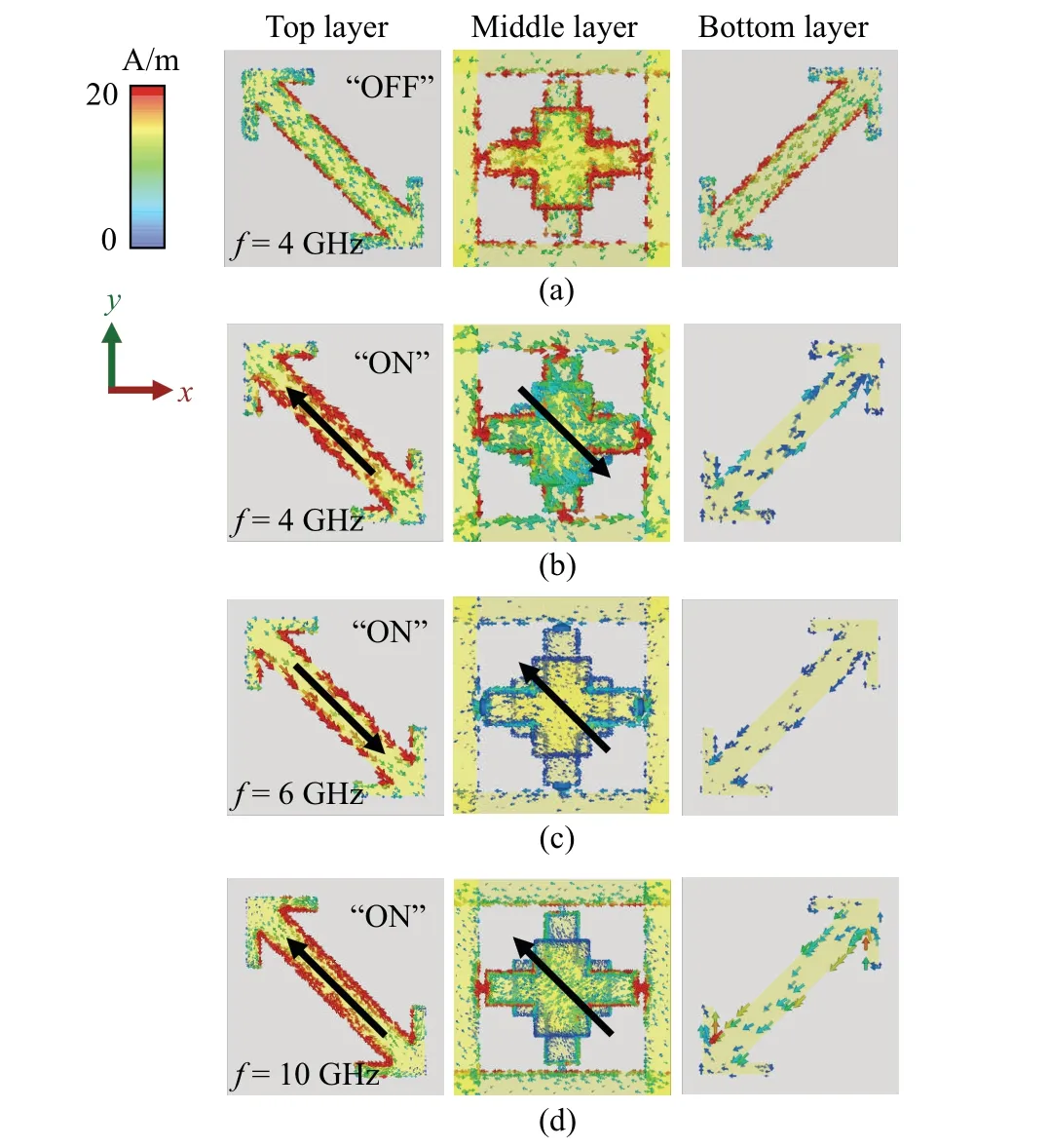
Fig.3.Surface current distributions on three layers of the proposed element(a)with diodes switched off at 4 GHz,and with diodes switched on at(b)4 GHz,(c)6 GHz,and(d)10 GHz.
As a proof of concept, a metasurface sample is then constructed with 2×2 two supercells assembled in a typical checkboard-like arrangement, and each of the supercells is composed of 10×10 identical basic elements.Normalized to a same-sized metallic plate,the scattering performances of the metasurface under a normal incidence are simulated and the results are shown in Fig.4.The backscattered field of the metasurface is obviously suppressed at 4 GHz when the PIN diodes are switched off within the frequency band of the transparent window,as evidenced by the comparison between Figs.4(a) and 4(d).This suppression occurs due to the efficient penetration of the incident energy through the metasurface.Moreover,at other out-of-band frequencies,the metasurface shows similar backscattering performances regardless of the working states of the PIN diodes.The backscattered energy is diffused into four oblique directions,thereby reducing the reflected energy in the normal direction and the monostatic RCS.
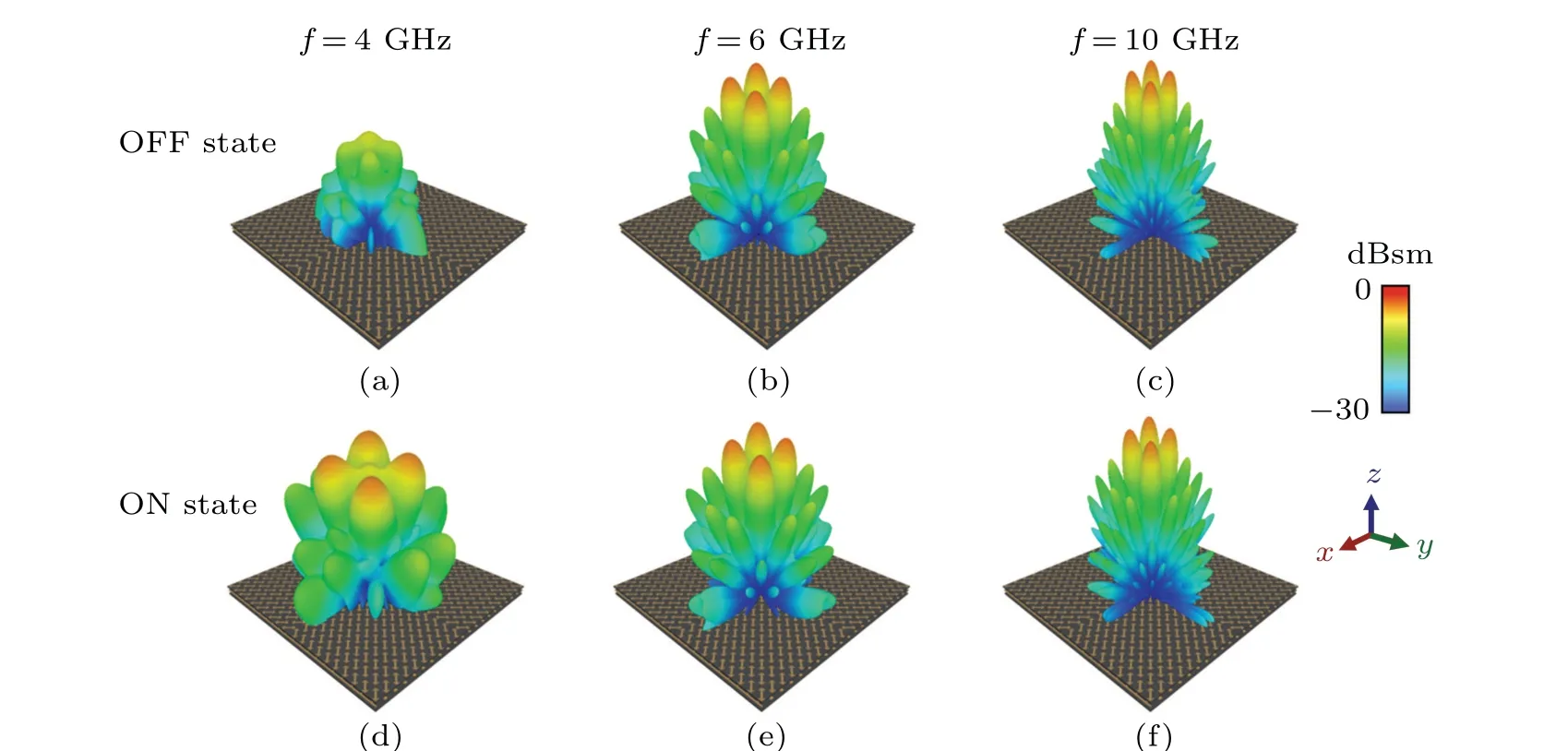
Fig.4.The simulated 3D scattering patterns of the metasurface normalized to the same-sized metallic plate under a normal incidence with diodes switched off at(a)4 GHz,(b)6 GHz,and(c)10 GHz,and with didoes switched on at(d)4 GHz,(e)7 GHz and(f)10 GHz.
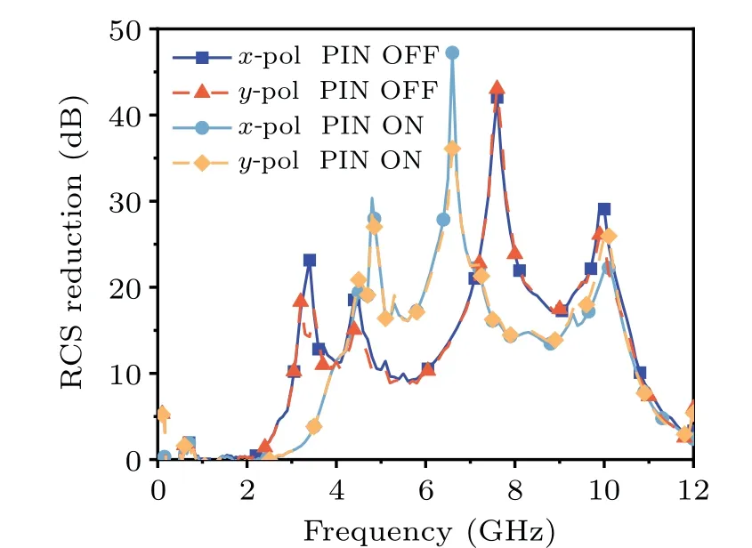
Fig.5.Simulated backward RCS reduction spectra for two biasing states under normal x-and y-polarized incidences.
Full-wave simulations based on the finite-difference timedomain(FDTD)method are performed to calculate the backward RCS reduction of the proposed metasurface, which is compared with a same-sized metallic plate.Figure 5 shows the RCS reduction spectra under the normal incident waves.Polarization insensitivity can be observed since the metasurface can realize broadband efficient RCS reductions for bothx- andy-polarized incidences.When the PIN diodes are switched on,the metasurface operates in the reflection mode,where a 180◦phase difference between the reflected fields will be generated by utilizing the checkerboard configuration and the polarization conversion performance, enabling the wideband RCS reduction.Consequently, the bandwidth of backward RCS reduction defined by 10 dB is from 3.8 GHz to 10.73 GHz (95.4% fractional bandwidth).On the contrary,when the diodes are switched off, the metasurface exhibits high-efficiency transmission at low frequencies and diffuse reflection at high frequencies, leading to a broader 10-dB RCS reduction bandwidth,which is observed in the frequency range from 3 GHz to 10.8 GHz(113%).
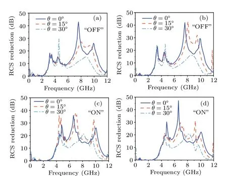
Fig.6.Simulated backward RCS reduction spectra under oblique incidences of (a) TE polarization and (b) TM polarization with diodes switched off, and (c) TE polarization and (d) TM polarization with diodes switched on.
To investigate the angular stability of the proposed metasurface, the RCS reduction spectra of the proposed metasurface for two polarizations under oblique incidences propagating in thexozplane is analyzed and provided in Fig.6.Here,TE mode is defined as that the incident electric field is perpendicular to the incident plane.While for TM mode, the incident electric field is parallel to the incident plane.As the incident angle increases from 0◦to 30◦, the RCS reduction level slightly reduces at some frequencies and the reduction bandwidth decreases.However,compared to a same-sized metallic plate, the wideband RCS reductions are still larger than 6 dB for TE-and TM-polarized incidences,regardless of the biasing state of the PIN diodes.
3.Measurements and discussion
To validate the simulated results,a prototype of the metasurface with 20×20 elements has been fabricated using the printed circuit board (PCB) technology, as shown in Fig.7.The three-layer structure is supported by a series of nylon screws that are positioned at the four edges,assuring the stability of the metasurface structure.Considering the space spared for the feeding network,the metasurface sample has an overall dimension of 350 mm×350 mm×14.5 mm.
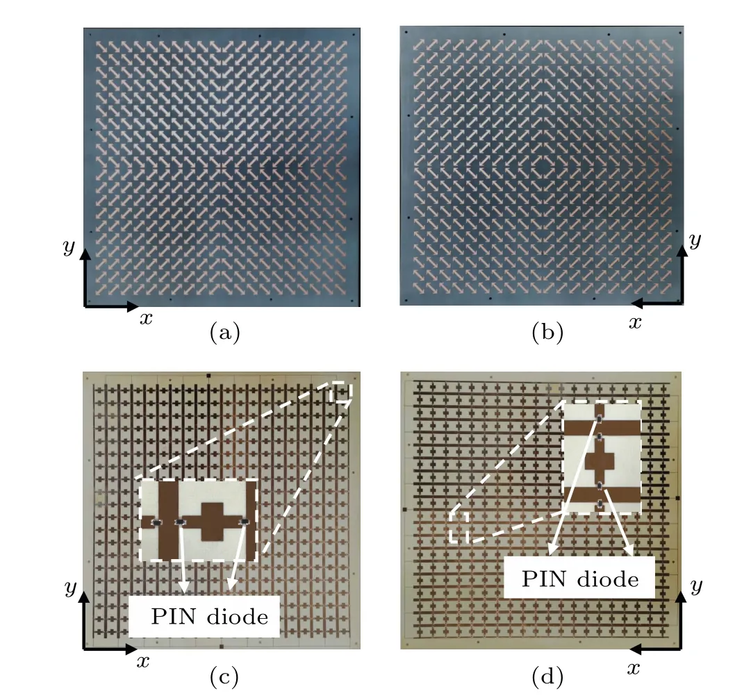
Fig.7.Photograph of the fabricated metasurface prototype.(a)Top layer.(b)Bottom layer.(c)Top and(d)bottom views of the middle layer.

Fig.8.Experiment setup to measure the characteristics of(a)RCS and(b)transmission of the proposed metasurface.
Figure 8 shows the schematic of experimental setup to measure the RCS reduction and transmission performances.To minimize the reflections from surroundings,the characteristics of backward RCS and transmissivity of the fabricated prototype are measured in a microwave anechoic chamber.By placing a pair of broadband linearly polarized horn antennas symmetrically about the metasurface or its normal plane,transmissivity or backward RCS can be recorded by a network analyzer(Agilent E8363A).The biasing voltage is controlled by a voltage source.
When measuring the scattering performance of the prototype,two horn antennas(one for transmitter and one for receiver)are assembled on a mechanical arc rail with a radius of 3 m.The oblique incidence angle is defined as the angle between the direction of transmitter(or receiver)and the surface normal of the MS sample,as shown in Fig.8(a).The RCS of a same-sized metallic plate is firstly measured as a benchmark to normalize the RCS of the prototype.Due to the characteristic of polarization insensitivity as shown in Fig.5,measurements are only performed for the case of ay-polarized incidence.Moreover,considering that most of the reflected waves would undergo polarization conversion, we also measure the crosspolarized scattering patterns on the diagonal plane of the proposed metasurface at 4 GHz and 7 GHz in the backward halfspace.In the experiment, the sample is placed in the center of the arc track,making the diagonal plane of the metasurface parallel to the arc rail.The receiving antenna is twisted by an in-plane angle of 90◦to measure the cross-polarized component, which can freely move along the arc rail to capture the scattered fields at different angles in the reflection space.
As illustrated in Figs.9(a) and 9(b), normalized to the same-sized metallic plate, both the simulation and measurement results indicate that the reflected wave will be split into four-beam with a maximum scattering power level below-6 dB, due to the destructive interference and the checkerboard distribution of the two basic elements.Moreover,most of the energy at 4 GHz can penetrate through the prototype when the loaded PIN diodes operate in the off state,causing a lower scattering power suppressed below-15 dB.The measured main beams are in good agreement with the simulation results except for a slight difference in beam widths, which may be caused by manufacturing and measurement errors.As shown in Figs.9(c) and 9(d), the measured 10-dB RCS reduction bandwidths are 3.9–9.7 GHz(85.3%)and 3–9.9 GHz(107%)for the on and off states,respectively,which agree well with the simulation results at the lower frequencies.However,since the maximum operating frequency of SMP1320-079LF PIN diodes is 10 GHz,the practical equivalent parameters are no longer equal to the value mentioned in Section 2 with the increase of frequency.In addition, limited by the insufficient sensitivity of the measured equipment, and the tolerance of fabrication,assembly,and experiments,there is a discrepancy between simulation and measurement for some peaks.Consequently,slight difference of red shift from 11 GHz to 10 GHz can be observed for the measured upper cut-off frequency of 10 dB RCS reduction.
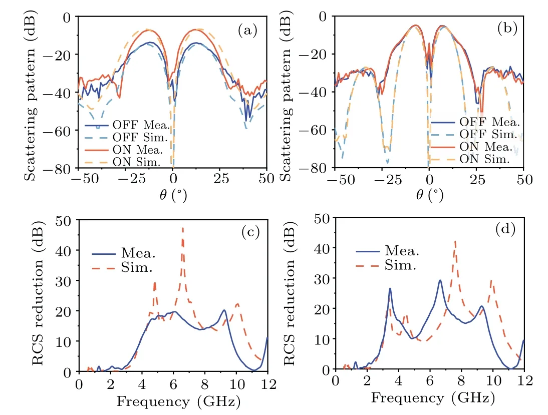
Fig.9.Simulated and measured cross-polarized scattering patterns on diagonal plane at (a) 4 GHz and (b) 7 GHz.Simulated and measured RCS reduction spectra with PIN diodes(c)switched on and(d)switched off.
Since the transparent window plays a pivotal role in metasurface design,we then measure the transmission performance of the metasurface prototype impinged by linearly polarized waves.As shown in Fig.8(b), the two horn antennas are placed symmetrically at the two sides of the prototype embedded in an absorbing screen with a distance of 2 m.The unity transmission is calibrated to the direct transmission between the two horn antennas.As shown in Fig.10(a),the measured results coincide well with the simulated ones,showing a highefficiency transmission greater than-3 dB from 2.76 GHz to 4.58 GHz when the metasurface with PIN diodes switched off is illuminated by ay-polarized incidence, and the maximum efficiency reaches 93%within the wide bandwidth.Moreover,the transmission coefficient is suppressed below-10 dB at 4 GHz when the diodes are switched on, which is very close to the predicted one.The slight frequency shift is attributed to the manufacturing tolerances,systematic errors in the measurement process and the difference between the actual and simulated diodes’parameters.Furthermore,Fig.10(b)shows the measured transmission results of the proposed metasurface underx-andy-polarized normal incidences,where the curves of the two polarizations are mostly overlapped,demonstrating the polarization insensitivity of the metasurface sample.
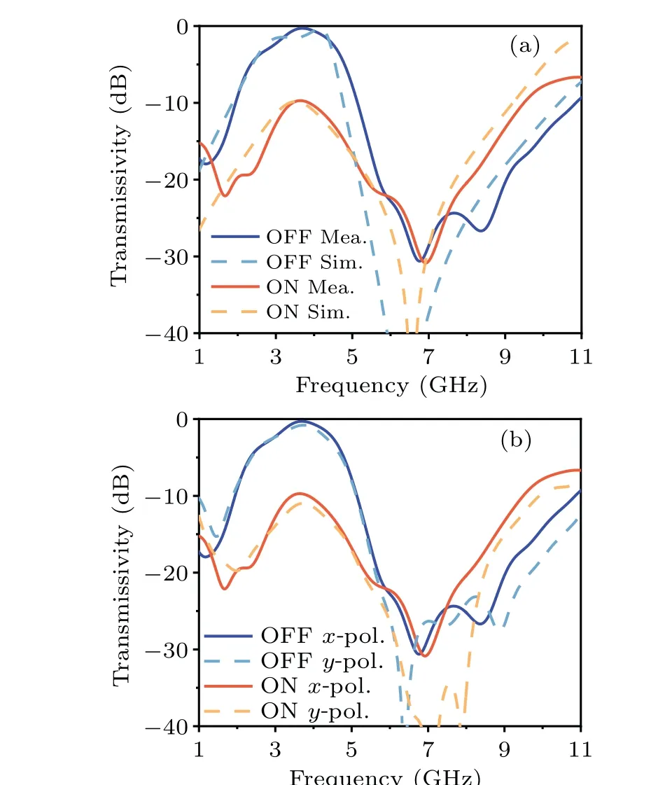
Fig.10.(a) Simulated and measured results of transmission performances at different biasing states.(b)Measured results of transmission performances for incidences with different linear polarizations.
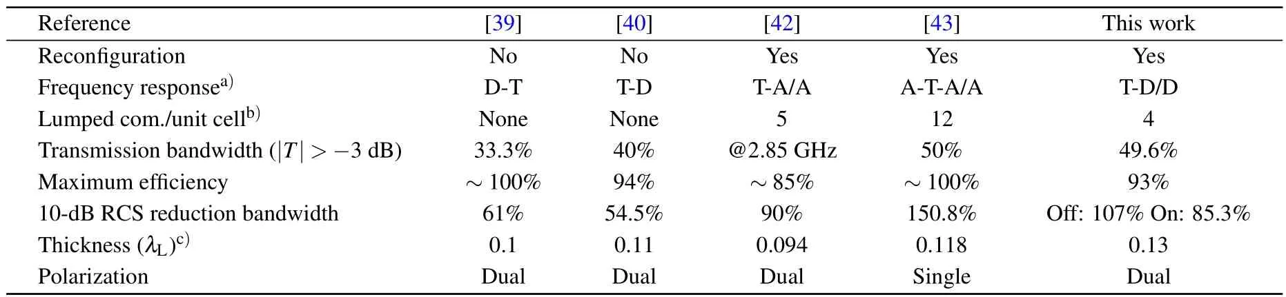
Table 1.Comparison with other low-scattering metasurfaces with a transparent window.
To clearly show the advantages of the proposed metasurface, we make comparison with some recent works on low-scattering metasurfaces with a transparent window in Table 1.Compared with the first two passive examples, our attempt achieves obviously broader bandwidths simultaneously with a switchable function for protecting the radiators in the transmission window.Different from the listed reconfigurable works employing absorption mechanism,the diffusion method used here not only reduces the number of lumped components,but also simplifies the design of the unit structure.Although a wider RCS bandwidth is shown in Ref.[43],the dual-polarized operation achieved in our work may find more application in practice.The proposed metasurface maybe used in stealth radar systems.On one hand,it can protect the system from being detected by enemy radar outside the band,and on the other hand, the working state between communication and stealth can be dynamically switched by changing the biasing states of positive components.In addition,the whole system may have the merits of low profile,low cost,and broad bandwidth.
4.Conclusion
In this article, a wideband low-scattering metasurface with an in-band reconfigurable transparent window is simulated,fabricated,and experimentally demonstrated.The metasurface consists of two layers of PCMs with a checkerboardlike configuration and a switchable FSS layer loaded with PIN diodes.By controlling the external bias voltage applied on the diodes, the metasurface can be flexibly switched between two different operation modes of high-efficiency transmission and low-scattering reflection within the tunable window.The proposed reconfigurable low-scattering metasurface does not require any extra biasing lines since the parallel strips in the transmission-reflection control layer can function as electrodes to provide DC bias voltages, successfully eliminating additional structural interference.In addition, our design has the advantage of polarization insensitivity due to the symmetrical structure.The experimental results are in good consistence with the simulated prediction.With the merits of switchable characteristics and broad bandwidth, the proposed strategy may promote the applications of metasurface in the development of stealth platforms and reconfigurable antennas.
Acknowledgements
Project supported by the Joint Fund of Ministry of Education for Equipment Pre-research(Grant No.8091B032112),the National Natural Science Foundation of China (Grant Nos.62271243 and 62071215), the Priority Academic Program Development of Jiangsu Higher Education Institutions,the Fundamental Research Funds for the Central Universities,and Jiangsu Provincial Key Laboratory of Advanced Manipulating Technique of Electromagnetic Wave.
猜你喜欢
今日农业(2022年16期)2022-09-22
鸭绿江(2021年21期)2021-08-17
晚晴(2020年7期)2020-12-03
财经(2020年14期)2020-08-02
华声文萃(2020年7期)2020-07-30
文萃报·周五版(2020年24期)2020-06-22
素质教育(2015年3期)2015-10-21
晚晴(2014年10期)2014-10-24
素质教育(2014年3期)2014-10-21
小天使·一年级语数英综合(2014年6期)2014-07-22

- Chinese Physics B的其它文章
- Unconventional photon blockade in the two-photon Jaynes–Cummings model with two-frequency cavity drivings and atom driving
- Effective dynamics for a spin-1/2 particle constrained to a curved layer with inhomogeneous thickness
- Genuine entanglement under squeezed generalized amplitude damping channels with memory
- Quantum algorithm for minimum dominating set problem with circuit design
- Protected simultaneous quantum remote state preparation scheme by weak and reversal measurements in noisy environments
- Gray code based gradient-free optimization algorithm for parameterized quantum circuit