
Databases of 2D material-substrate interfaces and 2D charged building blocks
2024-02-29 09:17JunDeng邓俊JinboPan潘金波andShixuanDu杜世萱
Chinese Physics B 2024年2期
Jun Deng(邓俊), Jinbo Pan(潘金波),2,3, and Shixuan Du(杜世萱),2,3,†
1Beijing National Laboratory for Condensed Matter Physics,Institute of Physics,Chinese Academy of Sciences,Beijing 100190,China
2School of Physics,University of Chinese Academy of Sciences,Beijing 100049,China
3Songshan Lake Materials Laboratory,Dongguan 523808,China
Keywords: 2D material-substrate interfaces, charged building block database, functional-oriented materials design,layered materials,density functional theory
1.Introduction
Layered materials, which are assemblies of twodimensional building blocks with relatively strong internal bonds compared with those between adjacent layers,have ignited great enthusiasm in the materials science community due to their fruitful advantages.The weak interlayer coupling of layered materials provides unique degree of freedom to modulate their chemical and physical properties by exfoliation, intercalation, etc.[1]They also exhibit anisotropic electronic properties,which may facilitate their application in nonlinear optics,[2]mechanics,[3]etc.These layered materials can be classified into van der Waals (vdW) layered materials and ionic layered materials according to the interactions between layers.[3]In van der Waals(vdW)layered materials,the building blocks are charge neutral.While in ionic layered materials,the building blocks are charged and usually cannot exist independently.
Since 2017, plenty of vdW layered materials and their monolayer structures have been predicted.2D databases containing stability, electronic, magnetic, and optical properties are constructed subsequently.[4–6]These monolayers can not only exist independently but also can be stacked or twisted to form heterojunctions with emergent phenomena.[7–9]Substrates usually are templates for the synthesis of twodimensional(2D)materials,where the coupling between them could dramatically affect the intrinsic physical properties of the 2D materials.[10–12]The discovery of suitable substrates in experiment is however time-consuming and costly.Thus,it is quite demanding to predict configurations of 2D materials on substrates theoretically.
Ionic layered materials, in contrast to vdW layered materials, have stronger interlayer coupling.They are composed of 2D charged building blocks, and these 2D building blocks can be classified into different roles, i.e., functional layers that mostly determine the physical properties of the crystal, and charge compensating layers which provide carriers.Functional-oriented material design can be achieved by stacking different functional layers and charge compensating layers.[13,14]While,the accessible 2D charged building blocks are limited,which hinders the rational design of layered materials.
In this paper, we address the above issues and construct 2D material-substrate interface (2DMSI) database and a 2D charged building block database.We also show the application of 2D charged building block database in designing and searching for functional layered materials.
2.Data acquisition
For the 2DMSI database, we choose materials in Materials Project[15]and Computational 2D Materials Database(C2DB)[6]as input for substrates and 2D materials.For substrates,we cleave their bulk phase along a Miller index to gain a surface, and then twist them with different angles.For 2D materials, we also make superlattice for them with different angles.Next,we put different twisted 2D materials on different twisted substrates with commensurate lattice, generating different twisted configurations.Finally, by high-throughput density functional calculations, we optimize the constructed superlattices to gain their binding energies.We also extend 2D materials-substrates to 2D–2D material heterojunctions[Fig.1(a)].Details can be found in Ref.[16].
For 2D charged building block database, we adopt a developed topological scaling algorithm (TSA)[5]to identify these 2D building blocks from Materials Project (MP)database.[15]There are three steps to map out them.The first step is data cleaning.We keep those structures in MP with ICSD codes andEhull=0 eV/atom to guarantee the high quality of the database.The second step is utilizing TSA to identify the bonded networks.We create ann×n×nsupercell for a structure, build the distance matrixDfor the supercell and construct a bond matrixBaccording toD.When the bond length between atomiandj di j ≤k×(rcovi+rcovj), they are connected, wherercoviandrcovjare covalent radii for atomsiandj,[17]andkis a scaling parameter.Then we keep those bonded atoms as a network.The third step is identifying the dimension of the network.We build ann×n×nsupercell for the network and find the number of bonded networksNin the supercell.Ifn3/N=1,it is a zero-dimension(0D)cluster; ifn3/N=n,it is a one-dimension(1D)chain;ifn3/N=n2,it is a two-dimension(2D)layer.Finally, we keep 2D layers with a different nominal elemental ratio with parent as 2D charged building blocks [Fig.1(b)].Here, we identify 1208 ones in total from the MP database.
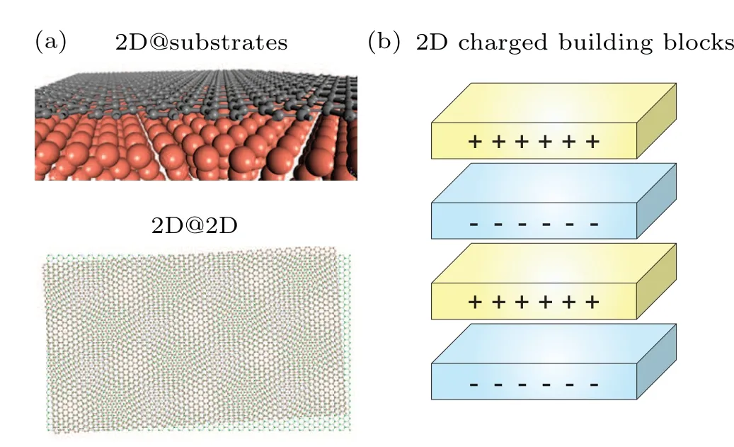
Fig.1.Schematic diagram of(a)2D materials-substrate interface(upper panel), twisted 2D–2D heterojunction (bottom panel), and (b) 2D charged building blocks.
We also build a workflow to construct layered materials by utilizing 2D charged building block database and identify 353 stable ones in terms of thermodynamics and latticedynamics by high-throughput calculations.In this work, we only consider 797 charged building blocks with tetragonal,trigonal and hexagonal symmetry as input.Then we stack them with commensurate lattice and charge neutrality.After constructing the layered structures, we resort to density functional calculations(DFT)to confirm their stability and investigate their physical properties.Details can be found in Ref.[18].
3.Data format and contents of the database
For the 2DMSI database,we provide an interactive webpage to exhibit our data as shown in Fig.2, which can be accessed via http://n11.iphy.ac.cn/databases/2dinterface.html.The “shape” button defines the lattice type of substrate and 2D material, which can be “hexagonal” or “square”.The“type” button can be “2D@substrate” or “2D@2D”, which correspond to interface between a 2D material and a substrate or between a 2D material and a 2D material.Then specify the detailed adsorbate and substrate.Next, define mismatch, max size, and max perfect square number of the supercell (PSN).Clicking “query” button will generate configurations of the superlattice.The bottom table shows the detailed information for each configuration, containing their superlattice matrixM, lattice constantl, mismatch∆, areaS,twisted degreeθ(◦), and binding energyEb.Here,Ebis defined asEb=(Ea+Es-Ec)/S, whereEais the total energy of adsorbate,Esis the total energy of substrate,andEcis the total energy of the composite superlattice.

Fig.2.Screenshot of interactive webpage for 2DMSI database.
Table 1.Contents for the json files.
For both 2D charged building block database and the designed layered materials, we provide a json format file for each entry, which is free to be read by multiple languages,e.g., python.For 2D charged building block database, each entry contains the basic lattice information, crystal structure,valence state,and its parent information.For the designed layered structures, each entry contains its energy, energy above hull, lattice information, crystal structure, band structure and phonon dispersions.Detailed information of the json file can be found in Table 1.We also provide python scripts to export the crystal structures, plot phonon dispersions and band structures,which are included in the database files.
4.Statistics of data properties
For the 2DMSI database,it contains data of 34 interfaces at present,including 6 2D@substrate entries,and 28 2D@2D entries.For each interface, there are usually 40–100 twisted configurations.
For the 2D charged building blocks, they are classified into 59 space groups (Fig.3).The most common one isP-3m1,which contains 287 entries in this subset.We also label functionality for part of building blocks based on the physical property of their parent compounds.
For the constructed 353 layered structures,they are classified into 30 space groups [Fig.4(a)].For their electronic structures,there are 52.1%non-magnetic(NM)metals,35.1%NM semiconductors, 6.8% magnetic metals and 5.9% magnetic semiconductors [Fig.4(b)].For semiconductors, their band gaps spread from 0–6 eV[Fig.4(c)].As a benchmark of utility of our databases for screening functional 2D materials,we present the discovery of 2D semiconductors with high carrier mobilities.According to the Drude model, the mobilityµof carrier can be expressed asµ=eτ/m*, wheree,τ,m*are the electron charge, scattering rate, and effective mass,respectively.Thus, the carrier mobility is inversely related to the effective mass.We firstly screen out those semiconductors with both low electron and hole mobility(|m*|≤0.2m0)as candidates, which yields 26 ones.Then those nonmagnetic semiconductors with direct bandgaps are considered for further processing.Then, we calculate their mobilities according to the deformation potential(DP)theory,[19,20]where¯his the reduced Planck’s constant,Cthe elastic constant,Elthe DP constant,kBthe Boltzmann constant,Ttemperature,andm*the effective mass,which can be extracted by DFT calculations.We find that 8 non-magnetic direct-bandgap semiconductors own high electron or hole mobility as shown in Table 2, which are potential candidates for application in high-speed electronic devices.
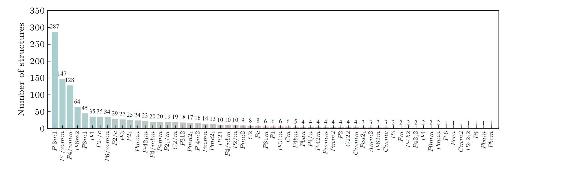
Fig.3.Statistics of space group for 2D charged building blocks.
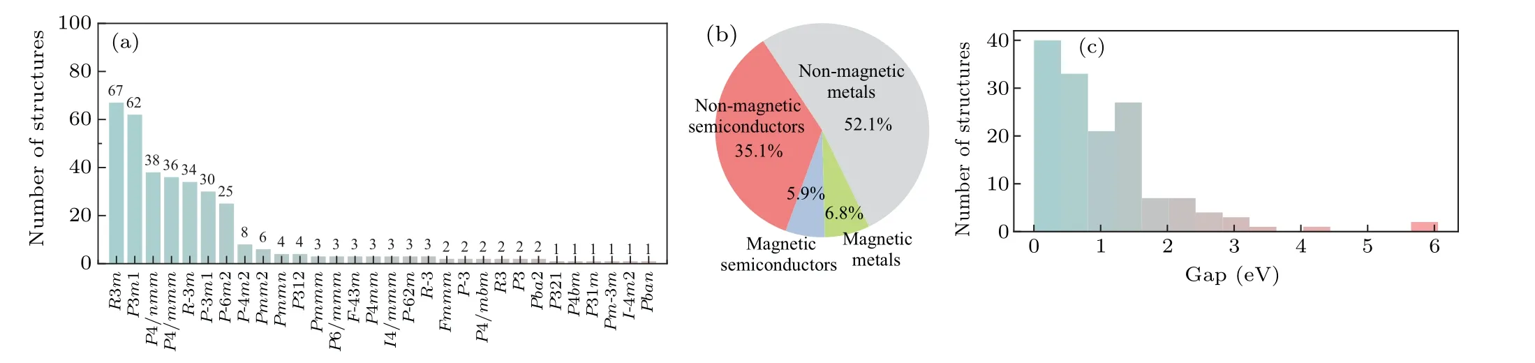
Fig.4.Statistics of(a)space groups,and(b)electronic structures for 353 layered structures.(c)Band gaps distribution for semiconductors.

Table 2.Computed carrier mobility of 8 non-magnetic semiconductors.
We also explore functionality of these materials.We find ferromagnetic semiconductor Na2CuIO6with valley Hall effect, superconductors CaAlSiF/Ba2F2PtAs, and topological material LaRhGeO,which is discussed in Ref.[18].
5.Conclusion
In this paper, we show detailed procedures to build the 2DMSI database and 2D charged building block database.For the 2DMSI database, we systematically study the possible configurations 2D materials at substrates or 2D materials,and provide an interactive webpage to exhibit our database.For the 2D charged building blocks,we have done its searching,classification and show its applications in designing and searching layered functional materials.This database and related layered structures are provided with json format, which can be extracted by python scripts that we provide.These databases provide a valuable resource to explore suitable substrate for 2D materials or 2D material heterojunctions and will serve as a valuable resource to construct functional layered materials.We will continuously expand the contents of the databases.
Data availability statement
The data that support the findings of this study are openly available in Science Data Bank at https://doi.org/10.57760/sciencedb.j00113.00188.
Acknowledgements
Project supported by the National Natural Science Foundation of China (Grant Nos.61888102, 52272172, and 52102193), the Major Program of the National Natural Science Foundation of China(Grant No.92163206),the National Key Research and Development Program of China (Grant Nos.2021YFA1201501 and 2022YFA1204100),the Strategic Priority Research Program of the Chinese Academy of Sciences (Grant No.XDB30000000), and the Fundamental Research Funds for the Central Universities.Computational resources were provided by the National Supercomputing Center in Tianjin.
- Chinese Physics B的其它文章
- Unconventional photon blockade in the two-photon Jaynes–Cummings model with two-frequency cavity drivings and atom driving
- Effective dynamics for a spin-1/2 particle constrained to a curved layer with inhomogeneous thickness
- Genuine entanglement under squeezed generalized amplitude damping channels with memory
- Quantum algorithm for minimum dominating set problem with circuit design
- Protected simultaneous quantum remote state preparation scheme by weak and reversal measurements in noisy environments
- Gray code based gradient-free optimization algorithm for parameterized quantum circuit