
A 10Gb/s combined equalizer in 0.18μm CMOS technology for backplane communication①
2015-04-17 05:33ZhangMingke张明科HuQingsheng
High Technology Letters 2015年2期
Zhang Mingke (张明科), Hu Qingsheng
(Institute of RF- & OE-ICs, Southeast University, Nanjing 210096, P.R.China)
A 10Gb/s combined equalizer in 0.18μm CMOS technology for backplane communication①
Zhang Mingke (张明科), Hu Qingsheng②
(Institute of RF- & OE-ICs, Southeast University, Nanjing 210096, P.R.China)
This paper presents a 10Gb/s high-speed equalizer as the front-end of a receiver for backplane communication. The equalizer combines an analog equalizer and a two-tap decision-feedback equalizer in a half-rate structure to reduce the inter-symbol-interference (ISI) of the communication channel. By employing inductive peaking technique for the high-frequency boost circuit, the bandwidth and the boost of the analog equalizer are improved. The decision-feedback equalizer optimizes the size of the CML-based circuit such as D flip-flops (DFF) and multiplex (MUX), shortening the feedback path delay and speeding up the operation considerably. Designed in the 0.18μm CMOS technology, the equalizer delivers 10Gb/s data over 18-in FR4 trace with 28-dB loss while drawing 27-mW from a 1.8-V supply. The overall chip area including pads is 0.6×0.7mm2.
analog equalizer, decision feedback equalizer (DFE), inductive peaking, current mode logic (CML)
0 Introduction
The rapid increase in transistor density and resulting routing complexity on serial links has made the data-rate per pin increased. However, bandwidth limited electrical channels, such as backplane or cable, introduce more losses as the data rate grows, these losses show that larger inter-symbol interference (ISI), which is the dominant factor for bit errors in high-speed links, challenges the communication quality. Therefore a more advanced signal processing circuit is required to overcome channels attenuation and improve sensitivity of the link[1].
Equalization circuit can compensate channel loss and suppress ISI, thereby recover the transmitted data. Traditional equalization circuit includes pre-emphasis equalizer, linear equalizer (LE) and decision feedback equalizer (DFE). Among them, both pre-emphasis equalizer and linear equalizer can compensate the attenuation of the channels by enhancing high frequency components, but they also amplify high-frequency noises and lower SNR. The nonlinear DFE, however, can reduce ISI from received data without amplifying noise and crosstalk, yet it only eliminates post-cursor ISI, while both pre-cursors and post-cursors ISI exist in a channel[2,3].
Based on the analysis above, this paper presents a 10GB/s combined equalizer for high speed backplane communication. By combing a linear analog equalizer with a nonlinear DFE, the proposed equalizer can well equalize the attenuation channel. This paper is organized as follows. Section 1 provides a review of backplane channel characteristics and a discussion of the equalizer architecture. Section 2 describes the circuit design in detail. The simulation and measured results are given in Section 3. Finally, Section 4 concludes the whole paper.
1 Architecture design
High speed signal transmission on FR4 backplanes is a challenge due to its heavy loss. Fig.1 shows the frequency response of an 18-inch trace on FR4 backplane with two advanced backplane connectors. Shown in Fig.1, the backplane channel exhibits a 28dB loss at 10GHz. To drive signals reliably through the backplane, normally an equalizer is needed to ensure the received signal not being distorted.
Fig.2 shows the block diagram of a proposed equalizer, in which a typical DFE combined with a conventional LE is constructed. Generally a DFE includes a slicer and an IIR filter, where N delayed outputs are fed back to the input with corresponding coefficients a1, a2,…,aN. Its primary function is to remove post-cursor ISI, while LE is responsible for suppressing pre-cursor ISI, as well as improves the ability of DFE.
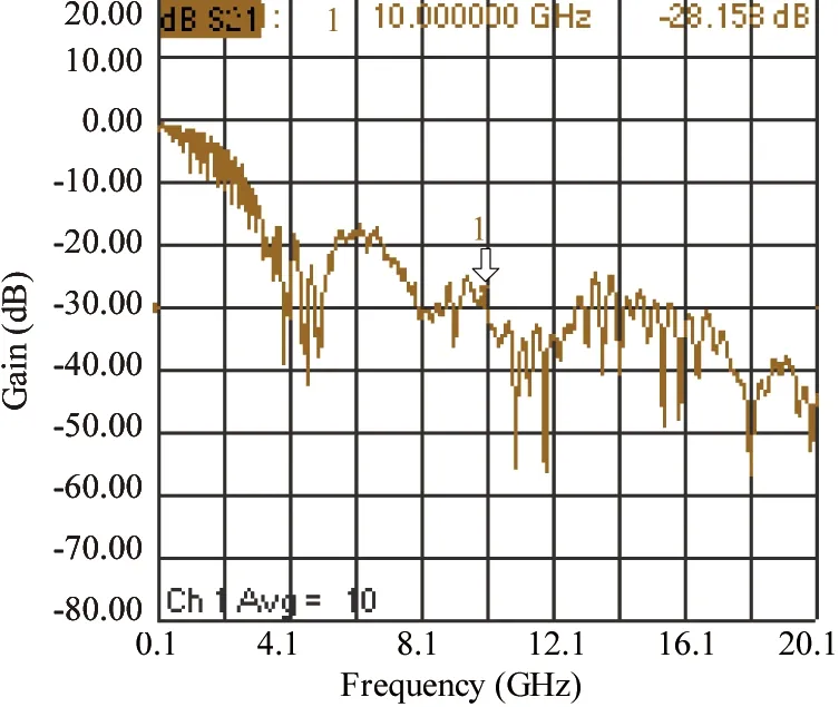
Fig.1 Channel frequency response of 18-inch FR4 backplane
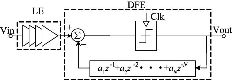
Fig.2 Block diagram of a combined equalizer
1.1 LE Architecture
LE can be implemented in two ways. One is to employ an FIR filter which is an architecturally flexible approach. Theoretically, the FIR filter can be designed to have a frequency response precisely equal to the inverse of the channel response and completely eliminate ISI in principle. However, its implementation requires precise analog delay elements[4], making it less practical, especially at higher data rates. Although low-loss transmission lines maybe used instead of active analog delay circuits, they are less practical in 18-inch or longer FR4 backplane trace which has higher loss.
Alternatives to FIR filter include conventional analog equalizer being composed of high-frequency boost circuits[5]. The locations of poles and zeros of the high-frequency boost circuits could be adjusted to fit a desired high-frequency boost in order to compensate channels loss. Because of its simplicity in implementation, such analog equalizer is used as a feed-forward linear equalizer in this work.
1.2 DFE Architecture
Many issues should be concerned to determine the architecture of DFE. Normally, there are two types of DFE: full-rate and half-rate architecture, shown as Fig.3. It can be seen that full-rate DFE only has one signal path, while the half-rate DFE contains two paths: the odd and even. Additionally, a MUX is needed to multiplex the two signals at the output. Therefor the full-rate DFE has smaller area and lower power consumption compared to the latter. However, the full-rate DFE has some drawbacks too. For example, D flip-flops (DFF) in it requires sampling bandwidth of full-rate (e.g.10Gb/s). Such a high speed DFF is a design challenge especially in 0.18μm CMOS technology because of the low characteristic frequency. Meanwhile, the Clk-to-Q delay of DFF must be considered accurately to ensure that the sampling point falls around the center of the input data eye. As a result, to achieve a more accurate full-rate clock, more clock buffers may be needed, increasing power consumption and area, especially for multi-tap DFE.

Fig.3 Full-rate and half-rate DFE
On the other hand, half-rate DFE has some advantages compared to full-rate DFE. First, this architecture can mitigate the speed limitations of the process by cutting the clock frequency in half[6], only at the cost of small increases in area and power consumption. Second, the clock buffer with small area can be designed easily, alleviating the total increase in area.
Another issue is to determine the number of DFE taps in order to make a tradeoff between area and gain. See Fig.2, for a current mode logic(CML) summer, a constant tail current in the output driver is required so as to keep a fixed common-mode level, this means the sum of all coefficients (the absolute values) is a constant[7]. Since the output is a feedback combination of all the (delayed) data inputs, the transfer function can be achieved from Vin to Vout as following:
(1)
Converting the discrete analysis above to continuous domain. It can be got:
(2)
where Tbis the bit period.
(3)
Eq.(3) holds when a1>0, a3>0, and a2=a4=…=0. In other words, if the total amount of all feedback coefficients is a constant (say K), the maximum boost at Nyquist frequency is also a constant regardless of the number of taps[7]. Fig.4 gives the comparisons of DFE responses using different taps with desired response. We can see that using three or more taps only improves the equalization quality, but not the amount of boosting, while increasing the area and power consumption.
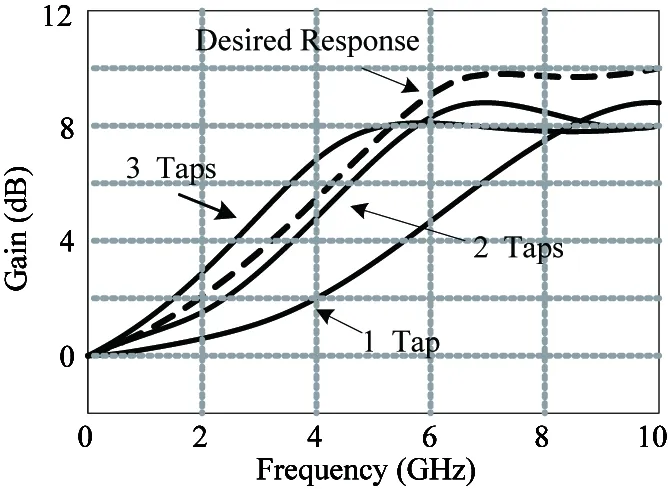
Fig.4 DFE responses with different taps
On the other hand, more taps may cause excessive parasitic capacitance at the output node of the CML summer. Thus the maximum data rate may roll off as the number of taps increases. Based on the analysis mentioned above, a 2 taps half-rate architecture is adopted in this paper to get a good trade-off between speed, area and power consumption.
Fig.5 shows the proposed equalizer architecture. Before DFE, an analog equalizer intersperses a high-frequency boosting filter with a gain buffer to provide a certain amount of boost, being used to remove the pre-cursor ISI and avoid amplifying the higher frequency noise or crosstalk. In the 2-tap half-rate DFE, the 10Gb/s input data is demultiplexed into two 5Gb/s signals odd and even by sampling a half-rate clock at both rising and falling edges. Then two half-rate data are delayed with DFFs, and the delayed versions are multiplied with the corresponding tap coefficients a1, a2. After that, the productions are fed back and summed at odd and even adders located in the input port. Actually, the multiplied results are subtracted from the input data at the adders to remove the post-cursor ISI. At the output, two half-rate outputs are picked up again alternatively into a 10Gb/s full-rate data by a 2:1 multiplexer (MUX).
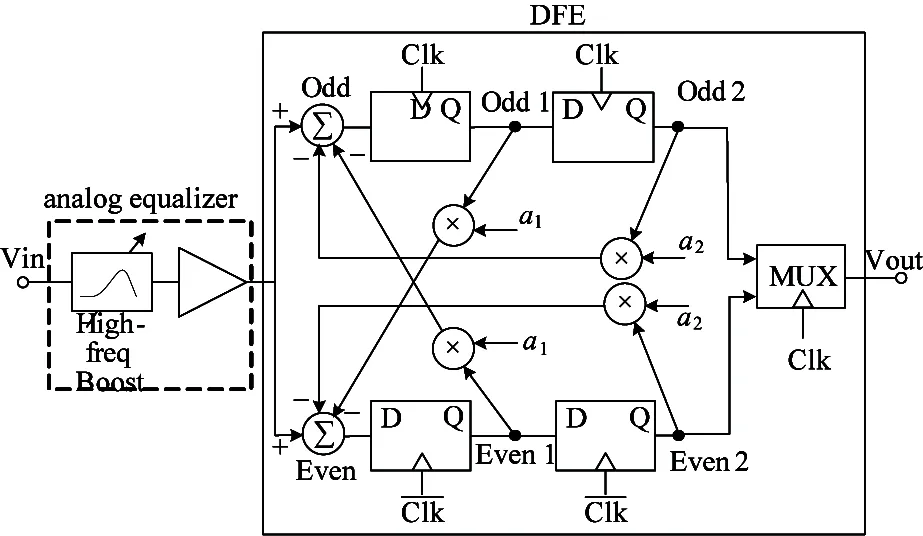
Fig.5 Block diagram of the proposed equalizer
2 Circuits design
2.1 High-frequency boosting filter
A conventional analog equalizer high-frequency boost circuit is RC-degenerated differential pair as shown in Fig.6. The parallel resistor-capacitor network RSCSyields a zero at ωz=1/RSCS, a dominant pole at ωp1=1/RDCLand a non-dominant pole at ωp2=(1+gmRS/2)/RSCS, where CSis the degeneration capacitance, RSis the degeneration resistance, RDis the load resistance and CLis the load capacitance, respectively. A zero introduces a +20dB/Decade rise in the frequency response, while a pole introduces a -20dB/Decade fall. Because of the limited gain-bandwidth product of the process, the dominant pole should not be much larger than the zero. As a result, for a high speed analog equalizer, only one zero can’t cancel pre-cursor ISI in the backplane channels with large loss.
To expand the overall bandwidth, the inductive shunt peaking techniques are utilized for improving the speed and gain without sacrificing the voltage headroom, shown as Fig.6. In Fig.6, nMOS transistors M3 and M4 act as degeneration capacitance, and M5 acts as a variable degeneration resistance along with M3 and M4, where the boost range and the gain of the analog equalizer can be adjusted by changing the control voltage. As the control voltage rises, the on-resistance M5 falls and so do the capacitances of M3 and M4, raising the magnitude of the zero[8]. Fig.7 compares the frequency responses of the boost circuits with and without inductive peaking. Obviously, by using the inductive peaking technique the bandwidth and the boost of the circuit are improved greatly compared to that of conventional one.
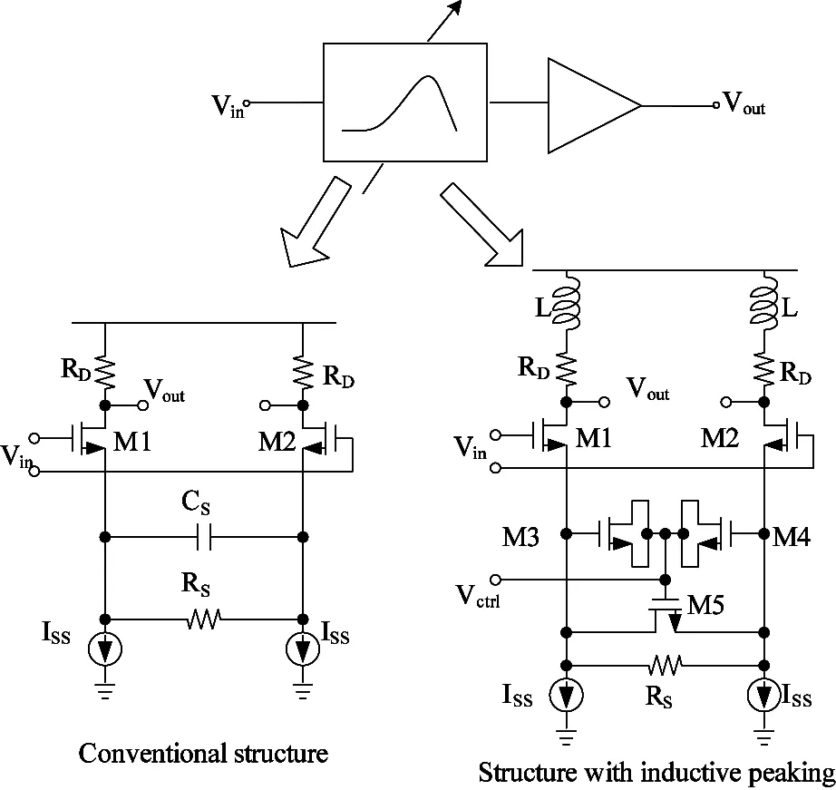
Fig.6 High-frequency boost circuit with and without inductive peaking
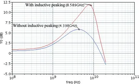
Fig.7 Frequency responses of high-frequency boost circuit
2.2 Multiplier and summer
The CML multiplier & summer at the DFE input is realized as series-gated differential pairs with common load resistors as shown in Fig.8. The Multiplication converts the input voltage of each differential pair into current, then the currents of each tap are added, where the tap coefficients a1add a2are dependent on the tail currents a1Issand a2Iss, which can be set based on the channel's pulse response off-chip.

Fig.8 Summer
2.3 D flip-flop
D flip-flop (DFF) in DFE serves as both storage element and slicer. As depicted in Fig.9, each DFF can be made with 2 cascaded latches running at opposite edges of half-rate clocks, of which the master latches the sampling input data at clock falling edge, and the salve one holds the data for one clock cycle.
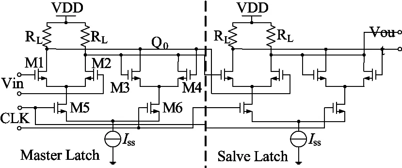
Fig.9 Schematic of CML-based DFF
It is well known that the speed of DFF is one of the key factors in improving the working frequency of circuit. For example, in the feedback path of the first tap, two main components are summer and DFF. Thus, to make the decision value be fed back and settled within one working period, following timing equation should be met[9]:
Tsummer+TDFF+Tprop≤UI
(4)
where Tsummerand TDFFare the delay of the summer and DFF, respectively. Tpropis the propagation delay of signal. From Eq.(4), it is known that when the input data rate is 10Gb/s, the total delay should be less than 100ps. Moreover, the DFF works as a slicing element too, necessitating a certain eye opening at its input for a desired BER. Hence, the DFF must exhibit a lower delay and high sensitivity.
Normally, DFF can be optimized by employing inductive peaking, as well as by reducing the sizes of transistors. The former method can effectively increase the bandwidth and reduce delay, but cause increase in chip area. Although small size is benefit to high speed, however, the transistor can not be too small. For example, when the sizes of cross-coupled pair M3, M4 are reduced below a certain critical value, they will not latch in the worst case. The sizes of tracking transistors M1, M2 and clock transistors M5, M6 should not be too small too, since these differential pairs need to be large enough to switch the current correctly[8]. Therefore, the choice of device dimensions is weigh designed to maximize the speed. A simulated eye diagram at one of the outputs of DFF is shown in Fig.10, showing a better eye opening. The simulated delay of DFF is only 50ps, which makes the overall delay of the feedback path equal to 77ps well below the UI of 100ps.

Fig.10 Simulated eye diagram at one of the DFF outputs
2.4 Multiplexer
The CML based 2:1 multiplexer (MUX) is shown in Fig.11. It is triggered by the same half-rate clock as DFF and works on both high and low levels of the clock. When the clock is enabled, clock transistors M5 and M6 work, selecting the odd and even data alternatively as the output. Although the MUX doesn’t participate in the feedback path, its speed is still crucial for DFE. This is because if the operating speed of the MUX is too slow, the two data paths can not be selected correctly, affecting the integrity of the output data.
乐学情境的创设,要求教师提供最佳的教学环境和活动场所;精心设计课堂教学的结构;有目的、有意识地制造教学高潮:把书本知识化为血肉丰满、生动活泼的形象;在教法上改变过去单一的”满堂灌”的注入式教法,将讨论式、对话式、辩论式、演讲式等教法引人课堂教 学,把学生带入探求新知的乐学情境,激发学生的学习兴趣。
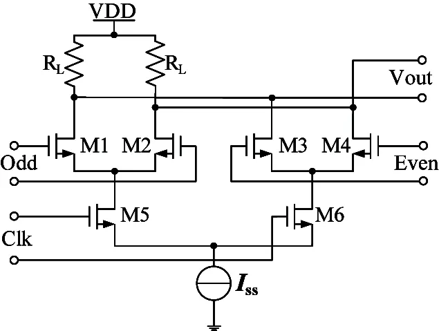
Fig.11 CML based MUX
Similar to DFF, the performance of MUX is also improved by reducing the sizes of transistors. The pole associated with differential pairs M1, M2 and M3, M4 is
(5)
where RS, CS, CGDand gmare the total resistance, capacitance, miller capacitance, and transconductance of the select pair, respectively. From Eq.(5), we learn that when gmbecomes small resulting from the size decrease of M1, M2 (M3, M4), the pole of the circuit will move to the right, thereby increasing the bandwidth. Different from that in DFF, however, in MUX the circuit losing latch which may appear when size of transistor is reduced too small, doesn’t need to be considered since there is no latch transistors at all. Of course, the minimum sizes of selected transistors are also needed to be ensured so that the circuit can switch the current correctly. Fig.12 shows the frequency response of MUX, it is seen that the 3dB bandwidth is improved by more than 2GHz from the original 7.6Hz to 10.1Hz.

Fig.12 Improved bandwidth of MUX
3 Measurement and results analysis
The proposed equalizer has been designed and fabricated in 0.18μm CMOS technology. Fig.13 shows the photograph of the equalizer. The overall chip area including a band-gap reference circuit, output buffer and pads is about 600μm×700μm.
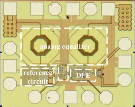
Fig.13 Photomicrograph of the proposed equalizer
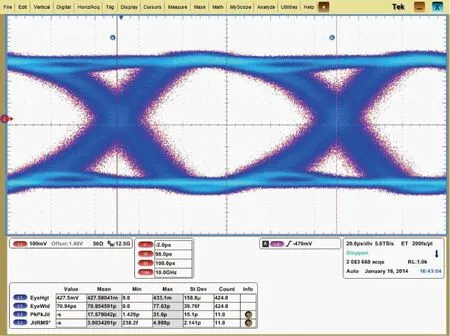
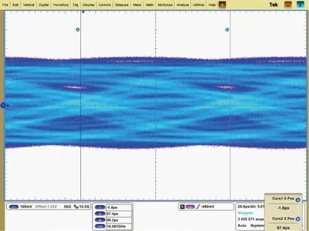
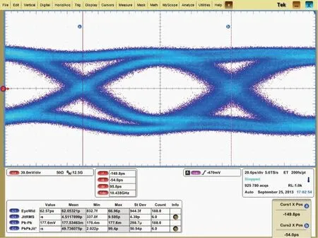
Fig.14 gives the block diagram of on-chip measurement for the equalizer. All measurements are performed on-wafer using high-speed GGB probes. Full-rate PRBS(pseudorandom bit sequence)15 data is generated using an Advantest D3186 pulse generator and pass through an 18-inch FR4 backplane channels, then send to the test chip, the outputs of the chip connect to an Tsktronix MSO 71254 oscilloscope to observe the signal eye diagram. A ballon is employed after the R&S SMP04 clock source to produce the half-rate differential clock required for the chip. Fig.15(a), (b) and (c) show 10Gb/s eye diagrams of original PRBS 15, the signal passing through 18-inch FR4 trace and the output of equalizer, respectively. We can see that the eye is almost closed after FR4 trace. After equalization, the majority of ISI is removed and the horizontal eye opening reaches 0.62UI, being almost the same as that of original eye diagram. This illustrates that the proposed equalizer works well at 10Gb/s.
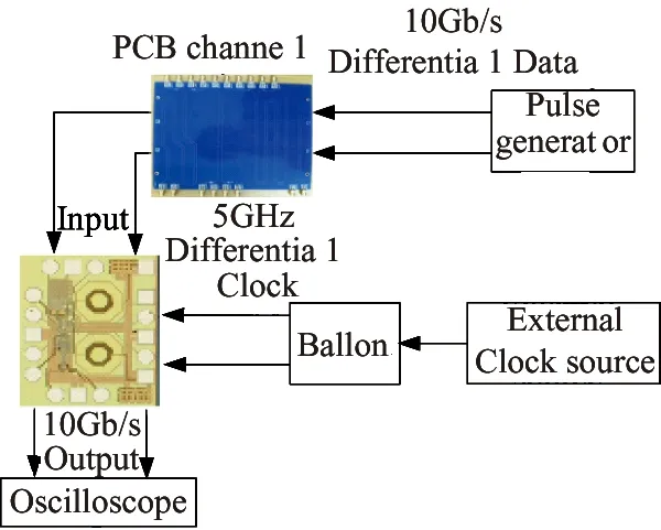
Fig.14 Block diagram of the on-chip measurement
Table 1 summarizes performance comparison of equalizers running at data rates around 10Gb/s. It can be seen that the proposed equalizer implemented in 0.18μm CMOS technology has higher data rate, lower power and smaller area compared with the 6.4Gb/s equalizer in Ref.[2]. While compared with Ref.[5] which uses the similar technology of 0.18μm, the proposed equalizer has higher speed of 10Gb/s. Although the rate of the equalizer in Refs[9] and [10] is not less than this work, they only eliminate post-cursor ISI and equalize the channels with up to 12dB at the 5.875GHz and 8.8dB loss at the 5GHz Nyquist frequency respectively, while the equalizer in this paper can cancel both pre-cursor and post-cursor and compensate 18dB channel’s loss.
(a) 10Gb/s PRBS signal
(b) After 8-inch trace
(c) Output of equalizer
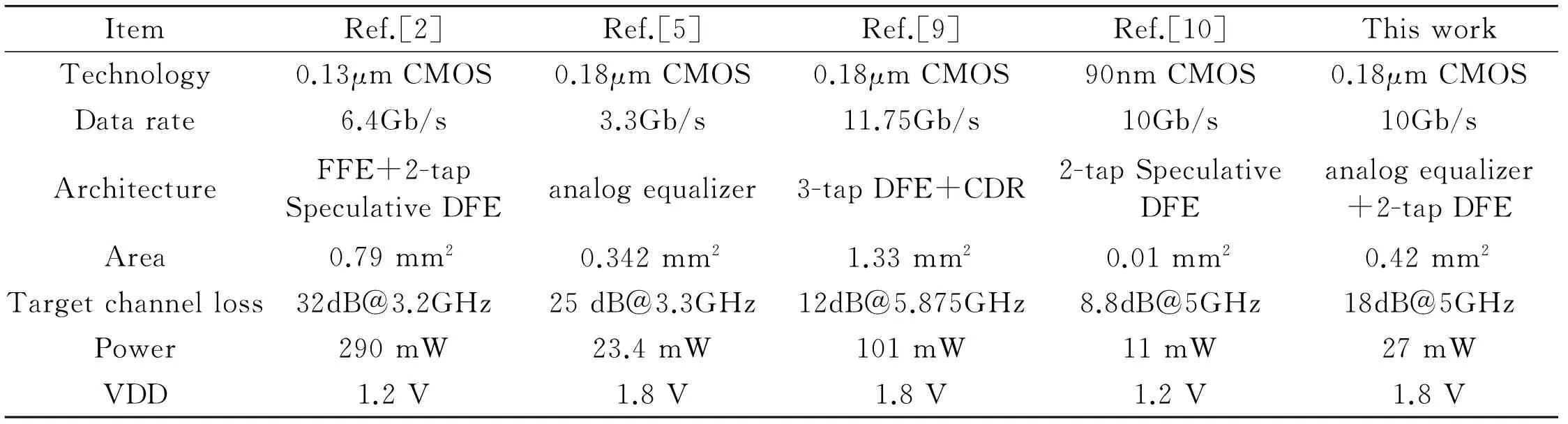
ItemRef.[2]Ref.[5]Ref.[9]Ref.[10]ThisworkTechnology0.13μmCMOS0.18μmCMOS0.18μmCMOS90nmCMOS0.18μmCMOSDatarate6.4Gb/s3.3Gb/s11.75Gb/s10Gb/s10Gb/sArchitectureFFE+2-tapSpeculativeDFEanalogequalizer3-tapDFE+CDR2-tapSpeculativeDFEanalogequalizer+2-tapDFEArea0.79mm20.342mm21.33mm20.01mm20.42mm2Targetchannelloss32dB@3.2GHz25dB@3.3GHz12dB@5.875GHz8.8dB@5GHz18dB@5GHzPower290mW23.4mW101mW11mW27mWVDD1.2V1.8V1.8V1.2V1.8V
4 Conclusion
In this work, a 10Gb/s combined equalizer is realized in TSMC 0.18μm CMOS technology. The equalizer composed of an analog equalizer and 2-tap DFE can cancel both pre-cursors and post-cursors with less noise enhancement and lower bit error rate. Measured results show that the equalizer chip can operate at data rates up to 10Gb/s with an improved horizontal eye opening of 0.62 UI through an 18-inch FR4 backplane channel. The equalizer including pads occupies 0.6×0.7mm2and consumes 27mW from 1.8V supply voltage.
[ 1] Sanquan Song, Vladimir Stojanovic. A 6.25 Gb/s Voltage-Time Conversion Based Fractionally Spaced Linear Receive Equalizer for Mesochronous High-Speed Links. IEEE J. Solid-State Circuits, 2011, 46(5):1183-1197
[ 2] T. Beukema, M. Sorna, K. Selander. A 6.4-Gb/s CMOS SerDes Core with feed-forward and decision-feedback equalization. IEEE J. Solid-State Circuits, 2005, 40(12):2633-2645
[ 3] T. O. Dickson, J. F. Bulzacchelli, and D. J. Friedman. A 12 Gb/s 11 mW half-rate sampled 5-tap decision feedback equalizer with current integrating summers in 45 nm SOI CMOS technology. IEEE J. Solid-State Circuits, 2009, 44(4):1298-1305
[ 4] MoonkyunMaeng, Franklin Bien, YoungsikHur. 0.18μm CMOS Equalization Techniques for 10-Gb/s Fiber Optical Communication Link. IEEE Transactions on microwave theory and techniques, 2005, 53(11):3509-3519
[ 5] Ju Hao, Zhou Yumei, and Zhao Jianzhong. A low power CMOS 3.3 Gbps continuous-time adaptive equalizer for serial link. Chinese Journal of Semiconductors, 2011, 32(9)
[ 6] Bret C. Rothenberg, Stephen H. Lewis. A 20-M samples Switched-Capacitor Finite-Impulse-Response Filter Using a Transposed Structure. IEEE J. Solid-State Circuits, 1995, 30(12):1350-1356
[ 7] Huaide Wang, Jri Lee. A 21-Gbs 87-mW Transceiver With FFE/DFE Analog Equalizer in 65-nm CMOS Technology. IEEE J. Solid-State Circuits, 2010, 45(4):909-920
[ 8] Srikanth Gondi, Behzad Razavi. Equalization and Clock and Data Recovery Techniques for 10-Gb/s CMOS Serial-Link Receivers. IEEE J. Solid-State Circuits, 2007, 42(9):1999-2011
[ 9] Lijun Li. Power Optimization of an 11.75-Gb/s Combined Decision Feedback Equalizer and Clock Data Recovery Circuit in 0.18-μm CMOS. IEEE transactions on circults and systems, 2011, 58(3):441-450
[10] Chang-Kyung Seong, Jinsoo Rhim. A 10-Gb/s Adaptive Look-Ahead Decision Feedback Equalizer with an Eye-Opening Monitor. IEEE transactions on circults and systems, 2012, 59(4):209-213
Zhang Mingke, born in 1985. He received his M.S. degrees in Integrated Circuits School of Southeast University in 2011. He also received his B.S. degrees from East China JiaoTong University in 2008. His research interests include the design of analog circuit, digital circuit and adaptive algorithms for equalizer.
10.3772/j.issn.1006-6748.2015.02.013
①Supported by the National High Technology Research and Development Programme of China (No. 2011AA10305)
②To whom correspondence should be addressed. E-mail: qshu@seu.edu.cn Received on Feb. 12, 2014
猜你喜欢
中学生数理化·中考版(2022年10期)2022-11-10
新教育时代·教师版(2020年18期)2020-08-10
商周刊(2018年15期)2018-07-27
新教育时代·教师版(2018年46期)2018-01-29
速读·中旬(2016年9期)2017-05-09
北方音乐(2017年4期)2017-05-04
课程教育研究·学法教法研究(2016年34期)2017-03-31
课程教育研究·学法教法研究(2016年36期)2017-03-31
福建中学数学(2016年8期)2016-12-03
发明与创新(2016年34期)2016-08-22
 High Technology Letters2015年2期
- High Technology Letters的其它文章
- MPLPK: A mobile path localization protocol based on key nodes①
- A method for retrieving soil moisture from GNSS-Rby using experiment data①
- Design and development of real-time query platform for big data based on hadoop①
- Research on suppress vibration of rotor misalignment with shear viscous damper①
- Security analysis of access control model in hybrid cloud based on security entropy①
- Improving wavelet reconstruction algorithm to achieve comprehensive application of thermal infrared remote sensing data from TM and MODIS①