ZnO纳米线阵列的电沉积法制备及表征
2010-12-12 02:42王丹丽阮永丰张灵翠杨红波
物理化学学报 2010年12期
王丹丽 阮永丰 张灵翠 杨红波
(天津大学理学院,天津 300072)
The multifunctional material ZnO has been used to make varistors,gas sensors,solar cells,and other devices since 1950s.It has attracted great interest recently in the semiconductor field[1-5]because of its large direct bandgap,strong exciton binding energy and important application prospects in optoelectronic devices. Most researches have been focused on its nanostructures and p-type doping[6-7],while few researches have been done on the luminescence of ZnO with non-p-n junction.It is possible to fabricate a new type of ZnO electroluminescence device with non-p-n junction by inserting ZnO into anodic aluminum oxide (AAO)templates[8].Based on the properties of AAO photonic crystals,the luminescence of ZnO in the device mentioned above would be enhanced[9].AAO has also been extensively used to synthesize nanometer-size fibril,rods,wires,and tubules through a variety of methods[10-11].Ordered ZnO nanowires play an important role in those applications.ZnO nanowire arrays were synthesized by one-step electrodeposition[12]in anAAO template. The deposition of Zn(OH)2introduced by aqueous solution competes with the formation of ZnO[13]and the Zn(OH)2can quench the near band emission of ZnO[14].Li et al.[15]also successfully prepared ZnO nanowire arrays in an AAO template through thermally oxidizing the Zn nanowire arrays in air. However,the thermal oxidation time was very long(about 35 h) and the deposited area was quite small.Because of the absence of suitable pretreatment of the AAO template,the challenge is to fabricate uniform ZnO nanowire arrays with large deposited area. Those drawbacks of the current methods to prepare ZnO/AAO assembly would limit its applications in electroluminescence devices.
In this paper,a more efficient method was developed to prepare large scale uniform ZnO nanowires.The oxidizing time was greatly decreased from 35 to 2 h and the deposited area of ZnO nanowire arrays was increased.Field emission scanning electron microscopy(FE-SEM),transmission electron microscopy(TEM), X-ray diffraction(XRD),and photoluminescence(PL)techniques were employed for sample characterization.
1 Experimental
TheAAO was fabricated by a two-step anodization process[16]. Briefly,a high purity(99.999%)aluminum plate was annealed at 550℃in air.After being electro-polished,the Al plate was anodized in 0.3 mol·L-1oxalic acid(>99.5%,analytical reagent, (AR))solution under constant voltage of 40 V at room temperature for 10 h.After removal of the anodic alumina layer,the texturedAl was anodized again under the same condition as the step one,and then theAl layer was removed in a saturated CuCl2(>99%,AR)solution.Asubsequent etching treatment was carried out in 5%(w)phosphoric acid(>85%,AR)solution at 30℃for 30 min to remove the barrier layer and enlarge the pore diameter. The thickness of the resultedAAO template is about 100 μm and the pore diameter is about 80 nm.
Ordered ZnO nanowire arrays embedded in AAO templates were fabricated by electro-depositing Zn followed by oxidation of the deposited Zn.Astandard three-electrode electrochemical cell was used for the electric deposition,with a saturated calomel electrode as the reference electrode,a Pt sheet about 3 cm2in area served as the count electrode.APt layer was placed by magnetron sputtering method onto one side of theAAO template used as the working electrode.Before mounting into the electrochemical cell, theAAO was immersed in an electrolyte solution under ultrasonic agitation for 10 min to remove the contaminants on the template surface and to improve the internal surface wettability.The treatment is critical to obtain homogeneous nanowires in the whole growing area.The deposition experiment was carried out in a solution containing 80 g·L-1ZnSO4·7H2O(>99.5%,AR)and 20 g·L-1H3BO3(>99.5%,AR)at room temperature for about 30 min.The voltage range was between 1.25 V and 1.30 V,and the time used was between 20 min and 30 min.The higher voltage was applied,the less deposition time was needed.After electrodepositing,the Zn nanowire arrays were embedded in theAAO. The subsequent step was to mechanically polish the Pt electrode, which was on the surface ofAAO.It is essential for Zn nanowire arrays to be oxidized sufficiently and efficiently.Through a thermal treatment in oxygen atmosphere at 800℃for 2 h,the deposited Zn was oxidized completely.The deposited Zn/AAO assembly was black with metallic luster.After oxidation,a white ZnO/AAO assembly was obtained.For FE-SEM study,the samples were quenched in liquid nitrogen for 1 min to obtain a regular cross section.For TEM observation,ZnO nanowires with theAAO template were dissolved in 1 mol·L-1NaOH solution to remove theAAO template and some dissociative ZnO nanowires were gotten.
2 Results and discussion
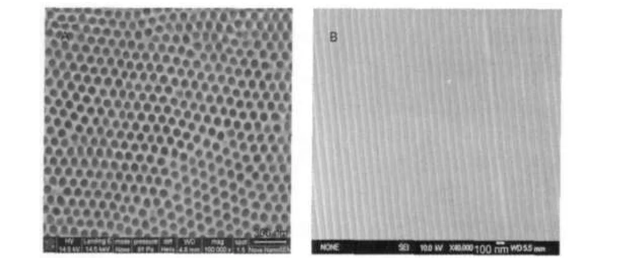
Fig.1 FE-SEM images ofAAO template(A)top view,(B)cross section view
The surface morphology and the structure of the AAO were observed by field emission scanning electron microscopy (FE-SEM NANOSEM 430,FEI,USA).As shown in Fig.1A, the AAO has a highly oriented porous structure of uniform pore sizes,which could be organized in a precise hexagonal structure.The average pore diameter of the AAO obtained is about 80 nm,while the interpore distance is about 120 nm. Fig.1B shows the FE-SEM image from cross section view of the AAO.It displays that the pore channels are nearly in parallel and the internal surface is smooth.
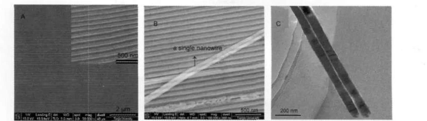
Fig.2 FE-SEM images of(A)ZnO nanowire array embedded inAAO and(B)a single nanowire out of the channel ofAAO, (C)TEM image of ZnO nanowiresThe inset in figureAshows the enlarged image of ZnO nanowire arrays.
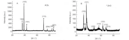
Fig.3 XRD patterns of the Zn nanowire embedded inAAO before(A)and after(B)calcination at 800℃for 2 h
Typical FE-SEM images of a ZnO/AAO assembly are shown in Fig.2A.It is observed clearly that the long ZnO nanowires uniformly embedded in AAO are of perfect straightness and continuity.The upper right inset is an enlarged magnification image of the ZnO nanowire arrays.It can be seen that the surface of the nanowires is smooth.The average diameter of the ZnO nanowires is about 80 nm,almost equals to the pore sizes of the template used.The nanowires are with very high aspect ratio of about 1000:1,with the length of about 100 μm,which equaling to template thickness.As can be noticed in Fig.2B,a single nanowire is out of the channel of AAO.It was formed when the sample was split for a cross section examination.Our data confirmed that the ZnO nanowires were compacted by the electrodeposition method.
To further confirm our experiment results,ZnO nanowires were also observed by transmission electron microscopy(TEM TECNAI G2F 20,PHILIPS).Fig.2C displays a result observed by the TEM.Two separate ZnO nanowires are shown in Fig.2C,and it is noticed that these nanowires are very straight, the diameter of these nanowires is about 80 nm,almost equals to the diameter of the nanochannels.
The crystalline structure was determined by XRD with Cu Kαradiation using a Rigaku X-ray diffractometer,as shown in Fig.3.Fig.3A shows the XRD pattern of as-deposited Zn/AAO assembly.There was no any other feature line in the sample but those of deposited Zn.Fig.3B shows the XRD pattern of the sample annealed in oxygen atmosphere at 800℃for 2 h. No Zn feature lines can be seen in Fig.3B,while ZnO phase was detected.It indicates that the Zn nanowires imbedded in AAO channels can be completely oxidized in 2 h under oxygen atmosphere condition.However,the same oxidation process would take 35 h in air.It shortens the preparation time of ZnO/AAO assemblies enormously by the electrodeposition method.Furthermore,the XRD patterns indicate that the ZnO nanowires are of polycrystalline structures without preferred orientation.We also found that there was Al2O3feature detected neither in Fig.3Anor in Fig.3B,which is because anodic aluminum oxide is amorphous until heated up to 824℃[17-18].
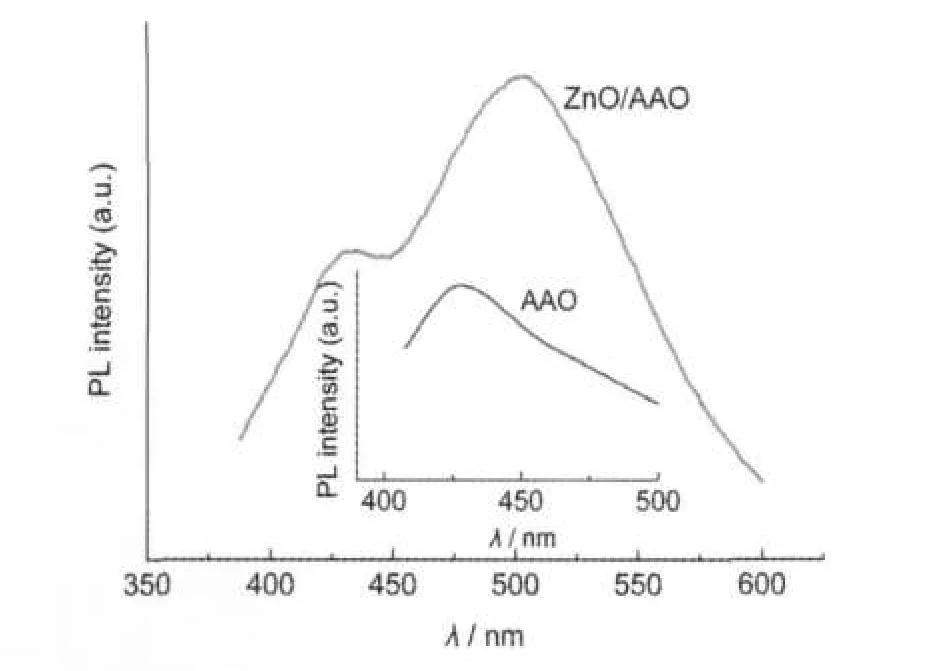
Fig.4 Photoluminescence(PL)spectrum of ZnO nanowiresThe inset is the PL spectrum of a blankAAO template.
Photoluminescence(PL212,SPEX)measurements were performed to study the luminescence property of ZnO nanowires. A strong emission band was observed at 504 nm,which was attributed to the oxygen vacancy defects of ZnO[19],as shown in Fig.4.A blue emission band at 430 nm was observed.Comparing the PL spectrum of a blank AAO template(the inset in Fig.4)with that of the ZnO/AAO assembly,we conclude that the broad emission band around 430 nm originates from the AAO template.
3 Conclusions
In conclusion,large scale uniform ZnO nanowire arrays based on hexagonally arranged AAO was fabricated by an effective electrodeposition method.Their FE-SEM images show that the ZnO nanowire arrays are long,continuous,and uniform.XRD patterns indicate that Zn nanowires in AAO can be oxidized completely in 2 h at 800℃ in oxygen atmosphere. The ZnO/AAO assembly has a strong green emission band at 504 nm and a blue emission band at 430 nm.The green emission is attributed to oxygen defects and the blue emission originates from AAO.The above conclusions suggest that the ZnO/ AAO assembly could be useful for the preparation of ZnO electroluminescence devices.
1 Serrano,J.;Manjón,F.J.;Romero,A.H.;Ivanov,A.;Cardona, M.;Lauck,R.;Bosak,A.;Krisch,M.Phys.Rev.B,2010,81: 174304
2 Wang,Z.H.;Geng,D.Y.;Han,Z.;Zhang,Z.D.Materials Letters,2009,63:2533
3 Willander,M.;Nur,O.;Zhao,Q.X.Nanotechnology,2009,20: 332001
4 Wang,X.Y.;Dong,G.F.;Qiao,J.;Wang,L.D.;Qiu,Y.Acta Phys.-Chim.Sin.,2010,26:249 [王小燕,董桂芳,乔 娟,王立铎,邱 勇.物理化学学报,2010,26:249]
5 Zheng,K.B.;Li,J.L.;Shen,H.T.;Sun,D.L.;Chen,G.R.Acta Phys.-Chim.Sin.,2008,24:1080 [郑凯波,李静雷,沈浩颋,孙大林,陈国荣.物理化学学报,2008,24:1080]
6 Silva,C.;Costa,A.R.G.;Cruz,M.M.;da Silva,R.C.;Borges, R.P.;Alves,L.C.;Godinho,M.J.Phys.-Condens.Matter,2010, 22:346005
7 He,H.;Lao,C.S.;Chen,L.J.;Davidovic,D.;Wang,Z.L.J.Am. Chem.Soc.,2005,127:16376
8 Ruan,Y.F.;Yang,H.B.;Jing,H.Q.;Lü,X.Y.The novel ZnO-based electroluminescent device prepared by usingAAO template:China,ZL200620027253.9[P].2007-9-12 [阮永丰,杨红波,井红旗,吕小燕.利用多孔氧化铝模板制作的氧化锌电致发光器件:中国,ZL200620027253.9[P].2007-9-12]
9 Wang,D.L.;Ruan,Y.F.;Yang,H.B.;Zhang,L.C.;He,L. Journal of Synthetic Crystals,2009,38:83 [王丹丽,阮永丰,杨红波,张灵翠,何 丽.人工晶体学报,2009,38:83]
10 Yang,L.;Tang,Y.H.;Chen,X.H.;Li,Y.;Cao,X.L.Mater. Chem.Phys.,2007,101:195
11 Wang,Y.C.;Ieu,I.C.;Hon,M.H.Electrochem.Solid-State Lett., 2002,5:C53
12 Zheng,M.J.;Zhang,L.D.;Li,G.H.;Shen,W.Z.Chem.Phys. Lett.,2002,363:123
13 Peulon,S.;Lincot,D.J.Electrochem.Soc.,1998,145:864
14 Zhou,H.;Alves,H.;Hofmann,D.M.;Kriegseis,W.;Meyer,B. K.;Kaczmarczyk,G.;Hoffmann,A.Appl.Phys.Lett.,2002,80: 210
15 Li,Y.;Meng,G.W.;Zhang,L.D.;Phillipp,F.Appl.Phys.Lett., 2000,76:2011
16 Li,A.P.;Müller,F.;Birner,A.;Nielsch,K.;Gösele,U.J.Appl. Phys.,1998,84:6023
17 Yue,S.;Du,J.;Zhang,Y.;Chen,D.P.Mod.Phys.Lett.B,2009, 23:3497
18 Kirchner,A.;MacKenzie,K.J.D.;Brown,I.W.M.;Kemmitt,T.; Bowden,M.E.J.Membr.Sci.,2007,287:264
19 Vanheusden,K.;Seager,C.H.;Warren,W.L.;Tallant,D.R.; Voigt,J.A.Appl.Phys.Lett.,1996,68:403
猜你喜欢
能源研究与利用(2022年3期)2022-06-27
西南科技大学学报(2021年4期)2022-01-15
人工晶体学报(2019年7期)2019-08-22
物理化学学报(2018年6期)2018-03-08
无机盐工业(2017年7期)2017-03-10
西华大学学报(自然科学版)(2015年3期)2015-07-18
物理化学学报(2015年5期)2015-02-28
物理化学学报(2013年1期)2013-07-25
物理化学学报(2013年5期)2013-07-25