
Application of real space Kerker method in simulating gate-all-around nanowire transistors with realistic discrete dopants∗
2017-08-30 08:26ChangShengLi李长生LeiMa马磊andJieRongGuo郭杰荣
Chinese Physics B 2017年9期
关键词:长生
Chang-Sheng Li(李长生),Lei Ma(马磊),and Jie-Rong Guo(郭杰荣)
Department of Physics and Electronic Sciences,Hunan University of Arts and Science,Changde 415000,China
Application of real space Kerker method in simulating gate-all-around nanowire transistors with realistic discrete dopants∗
Chang-Sheng Li(李长生)†,Lei Ma(马磊),and Jie-Rong Guo(郭杰荣)
Department of Physics and Electronic Sciences,Hunan University of Arts and Science,Changde 415000,China
We adopt a self-consistent real space Kerker method to prevent the divergence from charge sloshing in the simulating transistors with realistic discrete dopants in the source and drain regions.The method achieves efficient convergence by avoiding unrealistic long range charge sloshing but keeping effects from short range charge sloshing.Numerical results show that discrete dopants in the source and drain regions could have a bigger influence on the electrical variability than the usual continuous doping without considering charge sloshing.Few discrete dopants and the narrow geometry create a situation with short range Coulomb screening and oscillations of charge density in real space.The dopants induced quasilocalized defect modes in the source region experience short range oscillations in order to reach the drain end of the device. The charging of the defect modes and the oscillations of the charge density are identified by the simulation of the electron density.
electron transport,nanowire transistor,non-equilibrium Green’s function,dopant
1.Introduction
The control of electrostatic variability is increasingly important for metal–oxide–semiconductor(MOS)devices as the size continues to shrink.[1,2]In order to have an ideal gate control over the channel region,high-k oxides and tri-gate technologies have been employed in industry in the past few decades.For future MOS applications,full gate transistors, such as gate-all-around(GAA)nanowire MOS field-effect transistors,[3,4]attract significant interest due to their superior electrostatic gate control at ultimate-scaling.[5–7]However,the electrostatic variability associated with depleted impurities in the source and drain regions is still a major threat to further scaling and integration of nanowire MOS devices.[8–10]The statistical variabilities due to dopants or acceptors in the source and drain regions of nanowire MOS devices have been theoretically investigated by modeling various distributions, such as delta,[11]square well,[12]Gaussian,[13]and random distributions.[10,14–16]However,at a few nanometers,even though we call it highly doped,there are only a few impurities inside the device.The statistical analysis of various distributions could be inappropriate.Besides,the rapid technological achievement makes it possible to set arbitrarily the position of a single dopant inside nanowire devices.It is very relevant to consider a few impurities realistically inside the device and estimate the variance of the key electrical parameters.There have been several works on studying the influence of putting a single dopant or acceptor in a channel.[17]In further study,we need to simulate the variability introduced by a few realistic discrete donors arbitrarily added in the source and drain regions.Unfortunately,the potential of a dopant in the source or drain region has a substantial contribution to the total electrostatic potential at a narrow cross section and can easily break the ideal current characteristics.It also creates numerical difficulties of charge sloshing to achieve a reliable convergence in the self-consistent simulation.[8,9]
The charge sloshing problem is very common to induce numerical instability during the self-consistent iterations.[18,19]For ab initio molecular-dynamics simulations and electronic-structure calculations,particularly for inhomogeneous systems with large unit cells suffering from poor convergence,the Kerker method[20]is very efficient in preventing charge sloshing,especially in density functional calculations.[21–23]The original Kerker method[24]introduced by Manninen is applied in the reciprocal space,but it can also be applied in the real space and have the advantages of avoiding time-consuming integration to include the exponential kernel and be suitable for massively parallel computation.[25]Although the Kerker method is widely used in ab initio density functional calculations,it is relatively new in simulating MOS transistors,since we usually consider continuous doping in the source and drain regions and therefore no charge sloshing is incorporated.However,this approximation could miss some important physics at small size naowire devices since we include realistic dopants in the DFT calculation of molecular devices.In this work,we implement the real-space Kerker method self-consistently into a fully 3D real-space effective mass non-equilibrium Green’s function(NEGF)simulator for very narrow n-channel nanowire MOSFET with few discretedonors added in the source and drain regions and achieve the stable convergence.The realistic discrete dopants induced variations are also discussed.
2.Method
The dopant induced variation of electron density is treated by the usual self-consistent Schrödinger–Poisson procedure,[26]which is equivalent to the usual Hartree approximation.The Schrödinger equation within the effective mass approach is expressed as[27,28]
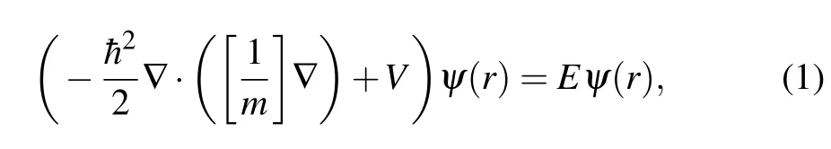
where[1/m]is the tensor of the inverse electron effective mass, ψ is the wave-function,and E is the energy.The electron–electron interactions are averaged through the dielectric constant ε.
When the effective masses are corrected from atomistic band structure calculations for each transverse cross-section, this self-consistent procedure is valid in simulating silicon nanowire transistors as narrow as 2 nm and the scattering is dominated by impurity scattering.[29–31]The electron–phonon scattering plays a minor role after appropriate fitting the values of the effective mass from full atomistic tight-binding band structure calculations.[16,32]The doping impurity is included by adding an on-site positive charge in the Poisson equation.For a general distribution with a continuous and discrete charge distribution,the Poisson equation coupled to the Schrödinger equitation is demonstrated in the form

where NDis the usual continuous doping function and n(r)is the electron density.The cjis the charge of a discrete doping atom located at position rj.For simplicity,we assume that the electrons and dopants are dominant charge carriers,the hole density and acceptors are neglected in this work.When we include random discrete dopants in the source and drain regions instead of assuming continuous doping,the dopants in the source and drain regions induce a numerical divergence from charge sloshing in the self-consistent Schrödingerpoisson loop.We adopt the real-space Kerker method to solve this problem.To demonstrate the real-space Kerker method, we transform the Poisson equation into a Helmholtz-like equation

where λ is the Thomas–Fermi wave vector.The Thomas–Fermi screening introduces a natural cutoff for the divergence.
The resulting solution is
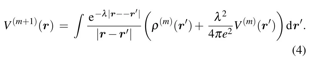
By transforming the Poisson equation into the Helmholtz equation,the charge sloshing problem is mainly solved since long range oscillations are naturally suppressed.
Once the self consistence of the Schrödinger–Poisson procedure is obtained,we adopt the Landauer–Büttiker transport method[33]based on the standard NEGF formalism[34]to calculate the transport properties.We define the Green function of the scattering region

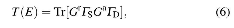
with

The drain current can then be calculated by the Landauer–Büttiker formula

HerefS(D)is the Fermi–Dirac distribution of the source(drain) defined as
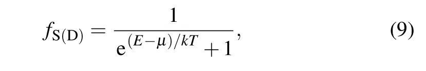
where k is Boltzmann’s constant,T is the absolute temperature,andµis the Fermi level.The total electron density of the system resulting from the electrons coming from the source and the drain can be calculated by the formula

The electron mobility is defined asµe=G/(eNtot),where G is the conductance defined by G=(2e2/h)T.
3.Results and discussion
The structure of the GAA silicon nanowire MOSFET along the transport direction is shown in Fig.1(a).The cross section of the nanowire is displayed in Fig.1(b).When the source and drain regions are assumed to be uniformly doped (NS=ND=1026m−3),the transmission coefficients with and without a single donor added in the middle of the channel are displayed in Fig.2.The intrinsic device without doping in the channel is characterized by the usual step shape.While the introduction of a single discrete donor in the channel generates dips below the steps in transmission,which implies that a donor could induce quasi-localized states.

Fig.1.(color online)The structure of the gate all around silicon nanowire MOSFET considered in this work:(a)the cross section in the x–y plane,(b)the cross section in the y–z plane,and(c)two discrete dopants in the source region,and another two dopants in the drain region along the central line.In all the calculations,the silicon body thickness is 2 nm,and the oxide thickness is 1 nm.
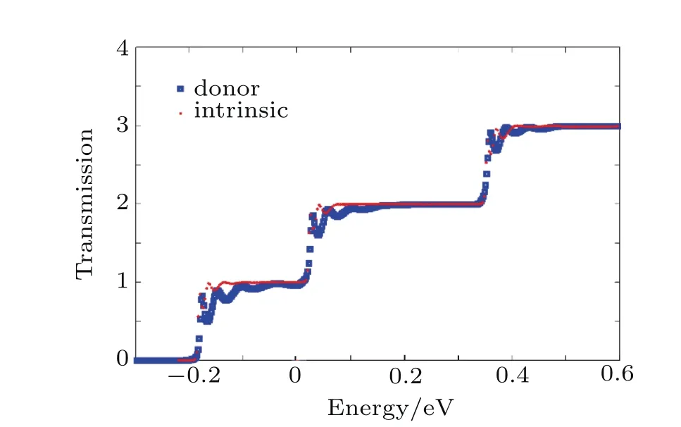
Fig.2.(color online)Transmission versus energy at V G=0.5 V for nanowire MOSFET with intrinsic(small red dot)and doped(big blue square)channel region.Here V DS=0.1 V.
In order to further investigate the effect of the donor, we vary the doping position from the source to the drain region.Figure 3 shows the mobility,conductance,and current as functions of the doping position along the central line of the nanowire.We notice that the fluctuations of conductance are relatively regular,no matter whether the discrete donor is added in the source,the channel,or the drain region.This is similar to the usual universal conductance fluctuation behavior.On the other hand,the mobility is higher when the donor is added in the source region compared to that added in the drain region.The reason could be that the single donor induced quasi-localized state is easier to be activated in the source than that in the drain due to the higher Fermi level in the source. When the donor is added between the source and channel regions,we can observe the largest mobility.The variation of the current with the doping position in the source and drain regions is more sensitive than that in the channel,as shown in Fig.3.
In order to further investigate the relation between the energy sub-bands and the doping position,we add four discrete dopantsin the source and drain regionsalong the centralline of the nanowire.For continuous doping in the source and drain, we observe in Fig.4(a)the usual sub-band structure.The drain voltage can be controlled accurately even at a short channel length.For four discrete dopants in the source and drain regions,we observe four sharp dips in Fig.4(b)corresponding to the donor positions in the source and drain regions.The energy positions and the charging of these states are extremely sensitive in the source and drain regions due to charge sloshing around the impurities.The attractive potential near the source region creates electron quasi-bound states,which can influence the mobility and the current flow.The sub-band profi le and therefore the currents cannot be accurately controlled as expected at narrow size.

Fig.3.(color online)(a)Electron mobility(in units of cm2/(V·s)),(b) conductance(in units of Ω−1),and(c)current(in units of A)versus the varied doping position of the single dopant added in the central line of the nanowire transistor.

Fig.4.(color online)The energy profile of the first sub-band along the central line of the silicon nano-wire(a)with continuous doping,and (b)with four discrete dopants added in the source and drain regions as shown in Fig.1(c).
We further show in Fig.5(b)that the electron density has short range charge sloshing in the doped source region before reaching the drain region at low gate voltage when the device is at the off region.This is quite different from the counterpart of continuous doping shown in Fig.5(a),where all defected modes are simultaneously activated in the source and drain regions without spatial delay.This implies continuous doping in the source and drain could underestimate the access resistance from dopants.Besides,we find that the defected modes are activated with short range charge sloshing and spatially related with the increase of the gate voltage in Fig.6.The short range charge sloshing and the way of mode by mode activating also indicate the quantum nature of the current.There could be a spatial delay in activating the doping defect modes for the realistic case compared to the continuous doping case.
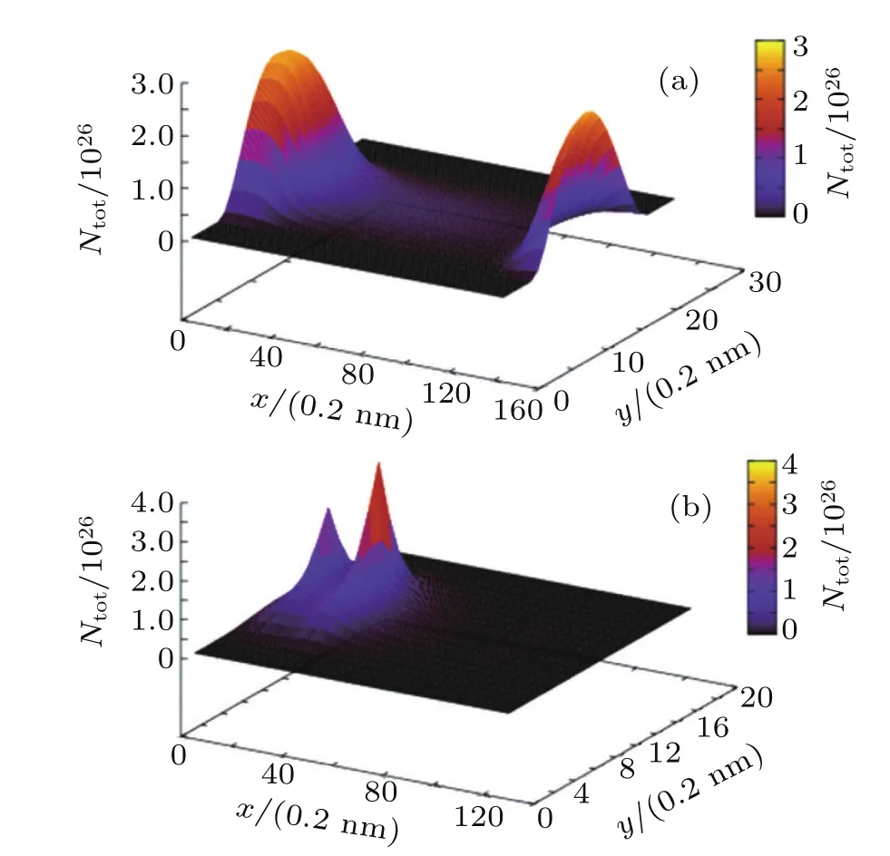
Fig.5.(color online)The electron density(in units of m−3)of a middle cross section for(a)continuous doping,and(b)four discrete dopants added in the source and drain regions as shown in Fig.1(c).Here V G=0.2 V and V DS=0.1 V.
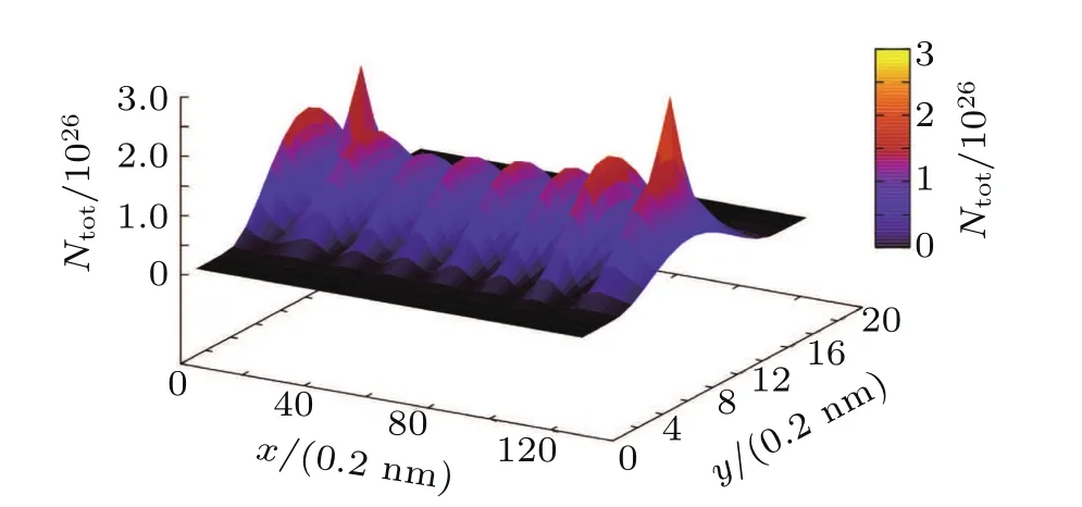
Fig.6.(color online)The electron density(in units of m−3)of a cross section with four discrete dopants added in the source and drain regions as shown in Fig.1(c)at V G=0.5 V and V DS=0.1 V.
4.Conclusion
We incorporate a real space Kerker method selfconsistently into our NEGF simulator.It has significant improvements in avoiding divergence over the usual Schrödinger–Poisson simulator when including discrete dopants in the source and drain regions.Realistic dopants could have bigger influences on the key electrical parameters than the case assuming continuous doping in the source and drain.The charging of doping defects in the source experiences oscillation and spatial delay before reaching the drain region at low gate voltage.The charging of realistic dopants and their short range oscillations of the charge density from the source to the drain region are essential to the large variability of the ultimate GAA nanowire transistors.
[1]Martinez A,Bescond M,Barker J R,Svizhenkov A,Anantram A,Millar C and Asenov A 2007 IEEE Trans.Electron Dev.54 2213
[2]Markov S,Cheng B and Asenov A 2012 IEEE Electron Dev.Lett.33 315
[3]Zhang L N,He J,Zhou W,Chen L and Xu Y W 2010 Chin.Phys.B 19 47306
[4]Liu Y,He J,Chan M,Du C X,Ye Y,Zhao W,Wu W,Deng W L and Wang W P 2014 Chin.Phys.B 23 097102
[5]Mayank C,Kinshuk G and Babu V G 2015 J.Nanosci.Nanoeng.Appl. 5 20
[6]Chen L,Cai F,Otuonye U and Lu W D 2016 Nano Lett.16 420
[7]Seo J H,Yoon Y J,Lee S,Lee J H,Cho S and Kang I M 2015 Current Applied Physics 15 208
[8]Seoane N,Martinez A,Brown A R,Barker J R and Asenov A 2009 IEEE Trans.Electron Dev.56 1388
[9]Martinez A,Seoane N,Brown A R,Barker J R and Asenov A 2009 IEEE Trans.Nanotechnol.8 603
[10]Yoon J S,Rim T,Kim J,Kim K and Baek C K 2015 Appl.Phys.Lett. 106 103507
[11]Bagwell P F 1990 Phys.Rev.B 41 10354
[12]Kim C S,Satanin A M,Joe Y S and Cosby R M 1999 Phys.Rev.B 60 10962
[13]Bardarson J H,Magnusdottir I,Gudmundsdottir G,Tang C S, Manolescu A and Gudmundsson V 2004 Phys.Rev.B 70 245308
[14]Mondal P,Ghosh B,Bal P,Akram M W and Salimath A 2015 Appl. Phys.A 119 127
[15]Nayak K,Agarwal S and Bajaj M 2015 IEEE Trans.Electron Dev.62 685
[16]Sylvia S S,Habib K M M,Khayer M A,Alam K,Neupane M and Lake R K 2014 IEEE Trans.Electron Dev.61 2208
[17]Georgiev V P,Towie E and Asenov A 2013 IEEE Trans.Electron Dev. 60 965
[18]Arias T A,Payne M C and Joannopoulos J D 1992 Phys.Rev.Lett.69 1077
[19]Kresse G and Hafner J 1993 Phys.Rev.B 48 13115
[20]Kerker G P 1981 Phys.Rev.B 23 3082
[21]Tassone F,Mauri F and Car R 1994 Phys.Rev.B 50 10561
[22]David R,Canning A and Wang L 2001 Phys.Rev.B 64 121101
[23]Marks L D and Luke D R 2008 Phys.Rev.B 78 075114
[24]Manninen M T,Nieminen R M,Hautojarvi P and Arponen J S 1975 Phys.Rev.B 12 4012
[25]Shiihara Y,Kuwazuru O and Yoshikawa N 2008 Modelling and Simulation in Materials Science and Engineering 16 3
[26]Tan I H,Snider G L,Chang L D and Hu E L 1990 J.Appl.Phys.68 4071
[27]Wang J,Rahman A,Ghosh A,Klimech Gand Lundstrom M 2005 IEEE Trans.Electron Dev.52 1589
[28]Bescond M,Autran J L,Munteanu D and Lannoo M 2004 Solid-State Electron 48 567
[29]Jin S,Tang T W and Fischetti M V 2008 IEEE Trans.Electron Dev.55 727
[30]Bescond M,lannoo M,Raymond L and Michelini F 2010 J.Appl.Phys. 107 093703
[31]Nehari K,Cavassilas N,Michelini F,Bescond M,Autran J L and Lannoo M 2007 Appl.Phys.Lett.90 132112
[32]Carrillo N H,Bescond M,Cavassilas N,Dib E and Lannoo M 2014 J. Appl.Phys.116 164505
[33]Datta S 1997 Electronic Transport in Mesoscopic Systems(Cambridge: Cambridge University Press)p.300
[34]Jauho A P,Wingreen N S and Meir Y 1994 Phys.Rev.B 50 5528
2 April 2017;revised manuscript
12 June 2017;published online 18 July 2017)
10.1088/1674-1056/26/9/097301
∗Project supported by the National Natural Science Foundation of China(Grant No.11104069).
†Corresponding author.E-mail:lcs135@163.com
©2017 Chinese Physical Society and IOP Publishing Ltd http://iopscience.iop.org/cpb http://cpb.iphy.ac.cn
猜你喜欢
小天使·一年级语数英综合(2021年6期)2021-08-09
——蓝田县北里村任长生家脱贫实录
金秋(2020年22期)2020-04-29
金沙江文艺(2019年2期)2019-11-13
基层中医药(2018年7期)2018-12-06
基层中医药(2018年3期)2018-05-31
新课程·中学(2017年4期)2017-06-29
意林(绘英语)(2017年6期)2017-02-17
河北书画研究(2016年1期)2016-08-24
创业家(2015年1期)2015-02-27
名作欣赏(2014年29期)2014-02-28

- Chinese Physics B的其它文章
- Improved control for distributed parameter systems with time-dependent spatial domains utilizing mobile sensor actuator networks∗
- Geometry and thermodynamics of smeared Reissner–Nordström black holes in d-dimensional AdS spacetime
- Stochastic responses of tumor immune system with periodic treatment∗
- Invariants-based shortcuts for fast generating Greenberger-Horne-Zeilinger state among three superconducting qubits∗
- Cancelable remote quantum fingerprint templates protection scheme∗
- A high-fidelity memory scheme for quantum data buses∗