
一种基于X射线成像的球栅网格阵列封装芯片焊接检测方法
2021-09-23 00:50:47冯辰越黄慧马燕
上海师范大学学报·自然科学版
2021年4期
关键词:数字图像处理
冯辰越 黄慧 马燕
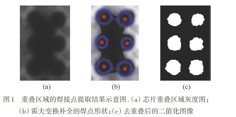
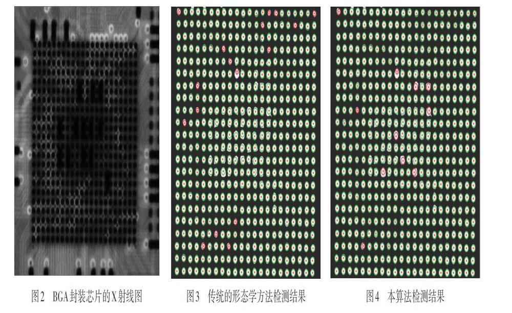
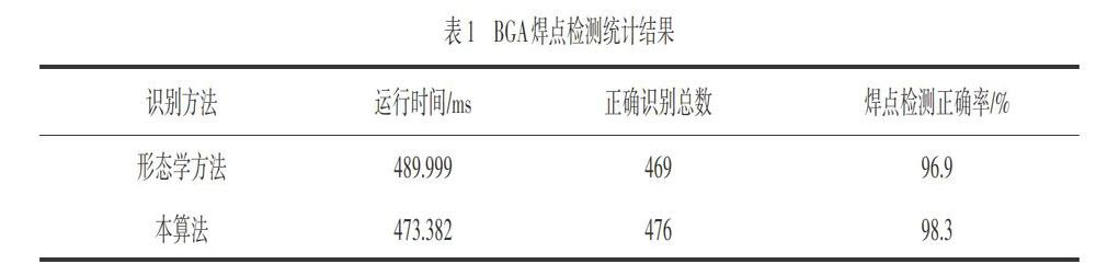
摘 要: 球栅网格阵列(BGA)封装芯片由于其引脚封装在内部的工艺特点,需要采用X射线成像的方式进行质量检查.提出一种基于印制电路板(PCB)X射线图像的自动芯片焊接质量检测方法,采用投影变换的方法确定芯片区域,根据球形焊点特点,利用霍夫变换对引脚焊点进行自动识别.该方法能实现全自动的焊接质量检查,提高焊点识别的效率和准确度,进而提高工业生产的效率和可靠性.
关键词: 印制电路板(PCB); X射线; 数字图像处理; 霍夫变换
Abstract: The ball grid array (BGA) packaging chip had to be detectedby X-ray image because of its internal pin package process characteristics. An automatic quality detection method of chip welding based on X-ray image for printed circuit board (PCB) was presented in this paper, which determined the chip area by the method of projection transformation. According to the characteristics of the spherical solder joints, the pin solder joints were recognized automatically by Hough transform. The proposed method could fully realize the detection of welding quality automatically and improve the efficiency and accuracy of the solder joints detection. Besides, the efficiency and reliability of the industrial production could also be improved.
Key words: printed circuit board (PCB); X-ray; digital image processing; Hough transform
0 引 言
与传统的封装方式相比,球栅网格阵列(BGA)封装方式具有更小的体积、更好的散热性能和电性能等优点,已成为高密度、高性能、多引脚封装方式的最佳选择.然而,BGA封装的I/O端子以圆形或柱状焊点的方式按阵列形式分布在封装的下方,芯片焊接普遍采用表面装贴技术,相比传统的印制电路板(PCB)焊接技术,会造成锡焊回流后PCB焊接质量难以检查的问题[1].X射线由于其具有较强的穿透能力,在质量检测[2-4]、安全检测[5-6]、健康检查[7-8]等领域,常被用于对物质内部进行无损探伤.在电路板焊接检测中,X射线成像也越来越被广泛地应用[9-13],但是目前生产线中还没有实现自动检测,而是借助于人工对照X射线图像辅助检测的方法[13],肉眼抽查X射线图像的内容,从而判断电路板是否有虚焊、短路等问题.这种方法受主觀因素的影响较大,并且效率和可靠度低,生产成本高.
目前基于X射线的BGA焊点检测研究,主……
登录APP查看全文
猜你喜欢
科技创新与应用(2016年34期)2016-12-23 16:04:22
电脑知识与技术(2016年28期)2016-12-21 11:35:19
中国科技博览(2016年25期)2016-12-20 19:41:38
电子技术与软件工程(2016年19期)2016-12-19 18:03:34
考试周刊(2016年91期)2016-12-08 22:19:28
中国教育信息化·基础教育(2016年9期)2016-10-18 02:49:16
大学教育(2016年9期)2016-10-09 08:58:06
电脑知识与技术(2016年6期)2016-06-06 14:29:07
科技视界(2016年3期)2016-02-26 10:11:04
光学仪器(2015年6期)2016-01-08 03:26:35