
Broad gain,continuous-wave operation of InP-based quantum cascade laser at λ ∼11.8µm∗
2021-12-22 06:42HuanWang王欢JinChuanZhang张锦川FengMinCheng程凤敏ZengHuiGu顾增辉NingZhuo卓宁ShenQiangZhai翟慎强FengQiLiu刘峰奇JunQiLiu刘俊岐ShuManLiu刘舒曼andZhanGuoWang王占国
Chinese Physics B 2021年12期
Huan Wang(王欢) Jin-Chuan Zhang(张锦川) Feng-Min Cheng(程凤敏) Zeng-Hui Gu(顾增辉)Ning Zhuo(卓宁) Shen-Qiang Zhai(翟慎强) Feng-Qi Liu(刘峰奇) Jun-Qi Liu(刘俊岐)Shu-Man Liu(刘舒曼) and Zhan-Guo Wang(王占国)
1Key Laboratory of Semiconductor Materials Science,Institute of Semiconductors,Chinese Academy of Sciences,Beijing Key Laboratory of Low Dimensional Semiconductor Materials and Devices,Beijing 100083,China
2Center of Materials Science and Optoelectronics Engineering,University of Chinese Academy of Sciences,Beijing 100049,China
3Beijing Academy of Quantum Information Sciences,Beijing 100193,China
Keywords: dual-upper-state(DAU),quantum cascade lasers,external cavity,gas detection
1. Introduction
Gas detection technology is widely used in environmental monitoring,medical diagnosis,drug detection,atmospheric science research and other fields.[1]A good light source for gas detection usually needs to meet the following conditions:Firstly, high output power for higher signal to noise ratio(SNR) and response rate of gas detection system; secondly,continuum-wave (CW) operation at room temperature (RT)for narrow laser linewidth, which can improve the stability and accuracy of the system; thirdly,broad tuning range to increase the variety of gas detections;fourthly,simple construction and portable size for gas sensing in complex monitoring environments.[2]Grating-coupled external-cavity (EC) QCL meets the above requirements and is an ideal light source for gas detection. The tuning range of EC–QCL mainly depends on the gain spectrum width of the active region,the reflectivity of anti-reflection(AR)coatings,grating diffraction efficiency,and so on. By the way, QCLs with broad-gain spectrum are not only suitable for gas detection, but also can be used for ultra-precision metrology and spectroscopy.[3]
Most trace gases of importance have characteristic absorption features between 3 µm and 17 µm wavelength.[4]QCLs in the wavelength range of 3.8–10.7µm have achieved watt-level CW output power at RT and are widely used in gas detection.[5,6]The wavelength range of 11–17 µm also covers the strong absorption peaks of NH3,C2H2,C2H4,benzene series pollutants, and even uranium hexafluoride.[2,7]However,the performance of devices in this spectrum area is much worse than that of 3.8–10.7µm devices due to the decrease of the internal quantum efficiencyηiand gain of core layers,the weakening of optical limit and the increasing free carriers absorption loss caused by the increased wavelength.[7–9]Beside,owing to the relatively higher electron effective massm∗e(the gain is proportional to (m∗e)–3/2),[10]it is more difficult for InP-based InGaAs/InAlAs QCLs with wavelength large than 11 µm to realize CW operation at RT when compared with InAs-based InAs/AlSb QCLs.[11,12]For these reasons, there were few studies on InP-based RT–CW–QCLs lasing above 11 µm in the past few years.[5,13]The longest wavelength(λ ∼11.5 µm) CW InP-based QCL with deep reservoir and double phonon resonance active design operating at RT was reported in 2008,showing a CW output power of 115 mW at 298 K, which is the highest CW output power of InP-based QCL reported atλ>11 µm so far.[14]However, the tuning performance of the device was not shown in Ref.[12]and the double phonon resonance design had little advantages in the broad gain of devices. In general, CW operation and broad gain are often incompatible, especially in the long wave region.While the Ref.[15]reported a InP-based QCL with dualupper-state (DAU) active design, and the tunable wavelength of the laser ranged from 9.5µm to 11.4µm in CW operation at RT, which provides a new method to fabricate broad gain RT–CW–QCLs atλ>11µm.[15]
Here, we reported CW operation of InP-based QCLs at 11.8 µm. In order to further expand the wavelength and achieve high performance, the modified dual-upper-state(DAU) active design was applied in devices for higher internal quantum efficiency and broad gain. Besides, optimized waveguide structure and buried heterogeneous(BH) process were also introduced for lower optical loss and better heat dissipation. Through the above methods, we finally fabricated broad gain RT–CW–QCLs atλ ∼11.8µm.
2. Active region design and waveguide structures
Active region layers of the devices reported here are consisted of lattice-matched In0.53Ga0.47As/In0.52Al0.48As quantum well barrier pairs, because the leakage current is no longer the main factor affecting the device performance when the wavelength is greater than 10 µm and ∆EC∼520 meV of the lattice-matched In0.53Ga0.47As/In0.52Al0.48As active region structure is considered to be enough to ensure confinement of carriers.[8]Besides, lattice-matched core layers can also reduce interface roughness induced scattering when compared with strain-balanced core layers,contributing to the better QCL performance.[16]The injectors are doped ton(Si)=1.4×1017cm−3for wider dynamic range of the injection current. In order to achieve RT CW QCLs ofλabove 11µm, it is necessary to improve the upper level lifetime, increase the extraction efficiency and suppress the carrier thermal backfilling. More importantly, a broad gain spectrum should also be designed to ensure the tuning performance of the device.
According to the above requirements,the QCLs presented here are based on a modified DAU active region design similar to that in an earlier paper,[17]where dual-upper states increase the combination of transitions between the upper and lower states and thus have a wide gain. Besides, lasers with DAU active region can be regarded as semi-indirect-pump(semi-IDP) lasers and the electron population in the injector is less than that of the conventional direct pump design,which improves the efficiency of population inversion process and reduces thermal backfilling carriers, resulting in the higher characteristics temperature.[18]In order to further expand the wavelength and achieve high performance,encouraging by the advantages of DAU active region design mentioned above,we try to modify the active region structure,and hope that devices can operate in CW mode and maintain a relative wide gain.
The schematic conduction band diagram and the relevant wave functions of the active region surrounded by two injector regions is shown in Fig. 1. By adjusting the thickness of the injected barrier layer close to the active region, the coupling strength between the higher upper state 5 and the ground state i′is improved. Strongly coupled 5 and i′improve carriers’injection efficiency,the maximum injection current and the peak of gain.[16]Besides, the wave functions overlap between the state 5 and parasitic 6-level wave functions is reduced,which reduces the leakage of carriers to the continuum.The energy diffidence between the two upper levels is small(E54∼18 meV),and carriers are easily scattered to the lower upper state 4 in various ways after tunneling from the ground state level i′to the higher upper level 5. Obviously, there are more electrons distributed in the lower upper state 4 in quantum wells where transitions occur. As a result, the transition processes associated with state 4 have larger transition matrix elements and the peak of optical gain near the emitting wavelength corresponding to state 4 is improved, making it easier for QCLs to operate in CW mode.
In addition, transitions (5–3, 5–2, 4–3, 4–2, 4–1) from the two upper levels to the quasi-continuous lower levels contribute to the broad gain. Transitions of the 5 to 3 and 4 to 3 are diagonal,which effectively increase the carrier lifetime of the two upper levels. The main transition (5–3, 4–3, 5–2, 4–2) matrix elementsZ53,Z52,Z43, andZ42and the upper laser levels lifetimeτ5andτ4are calculated to beZ53=1.5 nm,Z52= 1.1 nm,Z43= 1.91 nm,Z42= 1.9 nm,τ5= 2.0 ps,andτ4=1.2 ps. All of the above designs contribute to the broad gain and CW operation of InP-based QCLs lasing above 11µm.
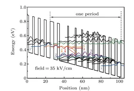
Fig. 1. Conduction band diagram and moduli squared of the relevant wave functions in the designed active region of the 11.8 µm QCL under an applied electric field of 35 kV/cm. The layer sequence of one active cell, given in nanometers and starting from the injector barrier, was 3.9/3.9/2.4/8.8/1.0/7.1/1.1/5.8/1.2/5.0/1.3/4.6/1.4/4.3/1.7/4.2/1.9/4.1/2.4/4.1/2.7/4.1, where In0.52Al0.48As barriers are in bold font,In0.53Ga0.47As wells are shown in normal font, and the underlined layers are doped(Si,n=1.4×1017 cm−3).
Detailed layer structures from the InP substrate up is shown in Fig. 2. InP buffer layers consisted of 2 µm InP(Si,4×1016cm−3)and 3µm InP(Si,2×1016cm−3)layers,which will reduce the series resistance between the substrate and the lower waveguide caused by the large doping concentration difference. A 3.9µm 50-stage laser core(Si,1.4×1017cm−3),a 300 nm InGaAs layer(Si,3×1016cm−3),a 3µm InP cladding layer(Si,∼3×1016cm−3),a 0.85µm graded doped InP layer(Si,∼1.5×1018cm−3) and 0.15 µm highly doped InP cap layer (Si,∼5×1018cm3) are followed. Highly doped cap layer can reduce surface plasmon-induced losses.[19]The full structure of the device is shown in Fig. 2. The metal organic chemical vapor deposition (MOCVD) is used for all layers’growth except for the active region and InGaAs layer, which are grown by molecular beam epitaxy(MBE).
3. Fabrication and characterization of the devices
A ridge-type BH structure was employed in this device for better heat dissipation, and semi-insulated InP: Fe with high thermal conductivity was grown on both sides of the ridge through selective epitaxy by MOCVD.The double channel ridge structure with an average ridge width of 16.5 µm was perpendicular to the direction of the crystal and fabricated by photolithography and wet chemical etching. Due to the anisotropy of two-dimensional materials, the device with the above ridge structure had higher transverse resistivity and less leakage and was beneficial to reduce the electrical loss. To further improve the heat dissipation and achieve higher output power, the device was mounted epi-side down on the diamond heat sink with indium and cleaved into chips of 3 mm,and the back facet was high-reflectance(HR)coated with ZrO2/Ti/Au/Ti/Al2O3.
The typical pulsed power–current–voltage(P–I–V)characteristics of heat-sink temperature are shown in Fig.3(a).The device is fixed on the water cooling platform with thermoelectric cooler (TEC) for heat-sink temperature control. The output power is directly measured by the pyroelectric power meter without lens collimation. The maximum peak output power in pulsed mode is up to 1.07 W under the duty cycle of 2% (10 kHz, 2 µs) and current of 2.4 A at 283 K. Based on the measuredP–I–Vdata under different temperatures,the threshold current density and slope efficiency of the device as functions of temperature are shown in Fig.3(b),the characteristic temperatureTis given to 255 K.Besides,the slope efficiency changes slowly as the temperature increases is similar to the Ref.[18],which is mainly caused by the resultant effect of both carriers’distribution in the injector and high injection efficiency.[18]
Figure 4(a)showsP–I–Vcurves under different duty cycle in 293 K, and the average power reaches 258.6 mW with a duty cycle of 50%. The device operated in CW is under the water and TEC cooling for temperature control, and CWP–I–Vcharacteristics are shown in Fig. 4(d). A maximum CW optical output power of 60 mW is measured at 293 K.Besides,we demonstrate the distinct dual-wavelength emitting (λ1∼11.8 µm,λ2∼11 µm) when current up to 1.9 A as shown in Fig. 4(c). Theλ2is generated by the transition of 5 to 2 and 4 to 1. In addition,we also measured electro-luminescent(EL) spectrum of the device under the subthreshold current and obtained a broad full width at half-maximum (FWHM)of 26.8 meV (2.37 µm), which is attributed to the transitions from the two upper states to the three quasi-continuous lower levels.
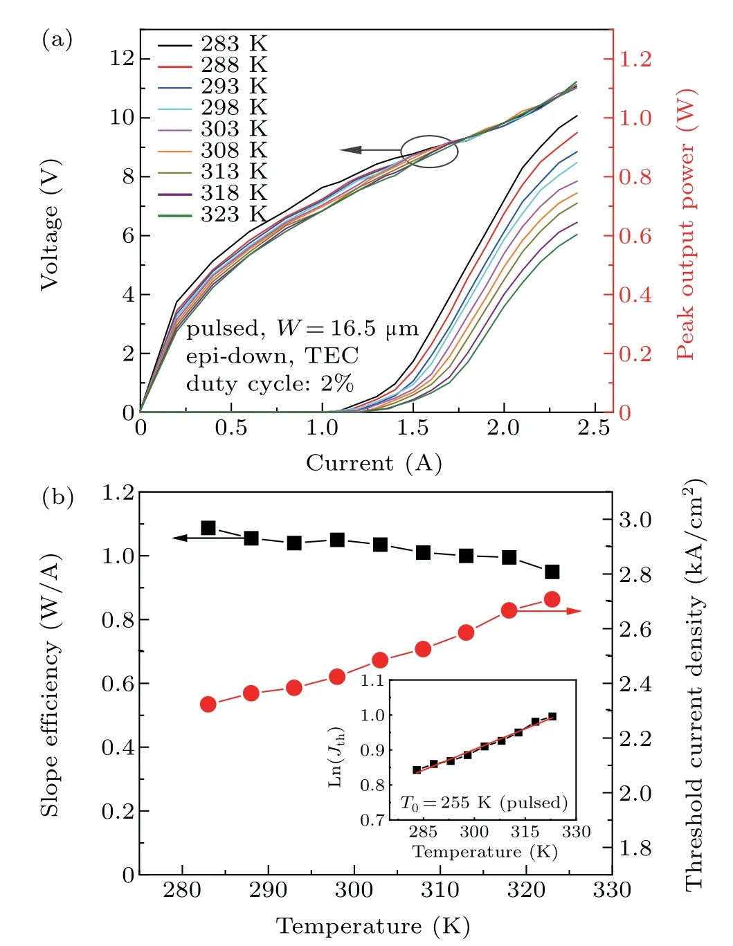
Fig.3. (a)Pulsed current–output power–voltage characteristics of a 3.0 mm long, 16.5 µm wide BH QCL under different heat-sink temperature. (b)Threshold current density and slope efficiency at threshold as functions of heat-sink temperature in pulsed operation. The inset in(b)shows the characteristic temperatures fitting curve of the device.
Similar to Ref. [20], the device with cavity length of 3 mm was fabricated to emitting on both facets with only the front facet AR (Al2O3/Ge) coated for higher external cavity feedback.[20]The EC–QCL system was chosen to be in Littrow configuration, which was consisted of two collimating lens, the QCL mentioned above and a blazed grating. Two lens were fixed on the front and back facets for beam collimating by ultraviolet curing adhesive,and the blazed grating was mounted on a rotation table controlled by a harmonic reducer motor to improve the grating rotation resolution. Based on the EC–QCL system of Littrow,we obtained the spectra and peak output power under different blazed grating angles as shown in Fig.6. A wide RT tuning range of 1.38µm(10.78–12.16µm)is measured under the duty cycle of 8% (40 kHz, 2 µs) and current of 1.6 A, which covers the strong molecular absorption lines of NH3and C2H2. And the maximum peak output power collected from the back facet(collimated through lens)of the EC–QCL is 71 mW corresponding to an emitting wavelength of 11.2µm under the same conditions.The AR coatings(Al2O3/Ge)we have mastered generate additional optical absorption in the above tuning range,so the tuning range will be further improved after improving the quality of AR films and changing the types of coatings,such as YbF3and ZnS.[21]
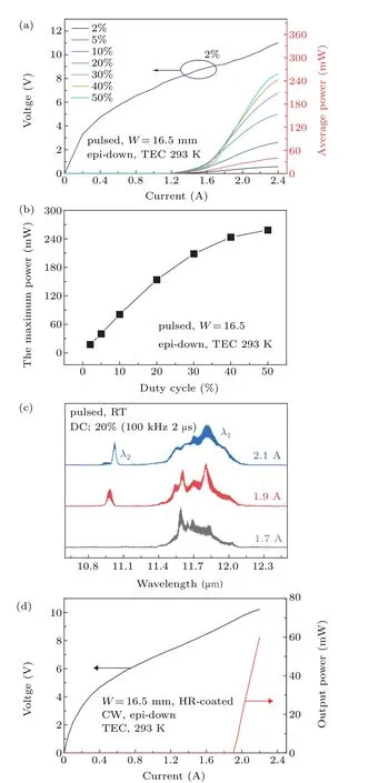
Fig.4. (a)Pulsed current–output power–voltage characteristics of a 3.0 mm long,16.5µm wide BH QCL at different duty cycle. (b)The maximum average power at different duty cycles. (c) Pulsed RT spectra of the QCL at different current. (d) CW current–output power–voltage characteristics of the device under water and TEC cooling at 293 K.
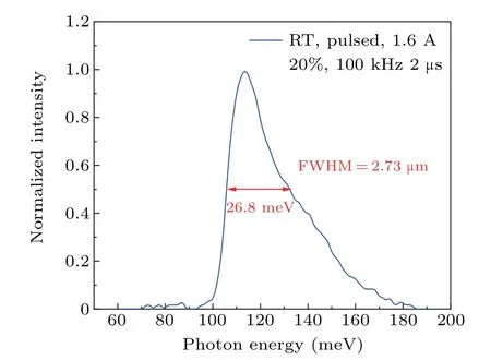
Fig.5. RT EL spectrum of the QCL mentioned above under the subthreshold current of 1.6 A with a duty cycle of 20%.
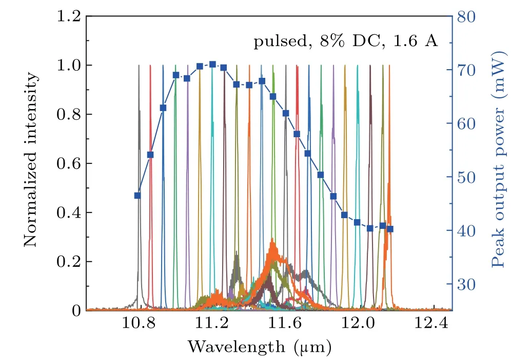
Fig. 6. Tuning behavior and peak output power of the EC–QCL. Measurements were taken at RT with a duty cycle of 8%(40 kHz,2µs)at 1.6 A.
4. Conclusion
A broad gain, CW operation QCL lasing at 11.8µm has been demonstrated based on the modified diagonal transition and dual-upper-state active region design. The peak power 1.07 W and 60 mW CW output power was obtained from a double channel buried ridge waveguide, 3 mm×16.5 µm(cavitylength×ridgewidth), HR-coated, 50 period QCL at 283 K and 293 K,respectively. The maximum average power was achieved up to 258.6 mW with a duty cycle of 50% and the characteristic temperatureT0was 255 K.Besides,a broad EL spectrum under the subthreshold current,the distinct dualwavelength emitting of the device in pulsed mode and a broad EC–QCL tuning range of 1.38 µm were demonstrated. In a word, the modified DAU-design devices appeared to be quite suitable for broadband tuning applications at long wave region.
Acknowledgement
The authors would like to thank Ping Liang and Ying Hu for their help in device processing.
猜你喜欢
中老年保健(2021年2期)2021-08-22
美与时代·城市版(2019年10期)2019-12-05
文艺生活(艺术中国)(2019年1期)2019-11-07
贵州农机化(2018年2期)2018-08-28
琴童(2017年4期)2017-06-14
小说月刊(2016年1期)2015-12-29
中国音乐教育(2014年6期)2014-05-16
外科研究与新技术(2011年2期)2011-08-15
青年文摘·上半月(1984年8期)1984-11-01
- Chinese Physics B的其它文章
- Transient transition behaviors of fractional-order simplest chaotic circuit with bi-stable locally-active memristor and its ARM-based implementation
- Modeling and dynamics of double Hindmarsh–Rose neuron with memristor-based magnetic coupling and time delay∗
- Cascade discrete memristive maps for enhancing chaos∗
- A review on the design of ternary logic circuits∗
- Extended phase diagram of La1−xCaxMnO3 by interfacial engineering∗
- A double quantum dot defined by top gates in a single crystalline InSb nanosheet∗