
Investigation of heavy ion irradiation effects on a charge trapping memory capacitor by C–V measurement
2023-10-11 07:55QiyuChen陈麒宇XirongYang杨西荣ZongzhenLi李宗臻JinshunBi毕津顺KaiXi习凯ZhenxingZhang张振兴PengfeiZhai翟鹏飞YoumeiSun孙友梅andJieLiu刘杰
Chinese Physics B 2023年9期
Qiyu Chen(陈麒宇), Xirong Yang(杨西荣), Zongzhen Li(李宗臻), Jinshun Bi(毕津顺), Kai Xi(习凯),Zhenxing Zhang(张振兴), Pengfei Zhai(翟鹏飞), Youmei Sun(孙友梅), and Jie Liu(刘杰),‡
1Institute of Modern Physics,Chinese Academy of Sciences(CAS),Lanzhou 730000,China
2School of Nuclear Science and Technology,University of Chinese Academy of Sciences,Beijing 100049,China
3Institute of Microelectronics,Chinese Academy of Sciences,Beijing 100029,China
4Lanzhou University,Lanzhou 730000,China
Keywords: charge trapping memory(CTM),high-k dielectric stack,heavy ion irradiation,reliability
1.Introduction
Non-volatile memories are one of the key components of modern electronic systems, which have important applications in the aerospace field.[1,2]Among all of the non-volatile memories, floating gate (FG)-based memories are the most widely used.With the increasing demand for device storage capacity and performance, the feature size of the memory cell is constantly decreasing.The FG structure faces many problems such as leakage current increase,parasitic coupling effects[3–5]etc.Charge trapping technology with oxide–nitride–oxide (ONO) or high-kdielectric stack structure was used to alleviate these problems.[6]Charge trapping technology can reduce the leakage current with the trapping layer,which has abundant traps to store charges separately.However,due to the limitation of the thickness of traditional tunnel oxide, the ONO structure also faces a trade-off between the erasing/programming speed and the data retention time.[7]The high-kdielectric stack structure relies on its small equivalent oxide thickness and rich charge trap density to improve the storage characteristics of the CTM.[8–11]Thus, the high-kdielectric stack structure is an important development direction of CTM technology.Many material systems,such as HfO2,[7]ZrO2,[12]HfAlO,[13]and SrTiO3[14]etc., have been reported to be utilized as the charge-trapping layers in a CTM capacitor.Among them,the HfO2/Al2O3/HfO2structure has received increased attention due to its advantages of good endurance,data retention,high speed,and so on.
There are many studies[15,16]on radiation effects on FGbased memories.It was reported that the charge loss in the floating gate induced by radiation would shift the threshold voltage of cell.This can seriously affect the reliability of devices.Compared to the FG structure, the ONO structure has better radiation tolerance.[17–19]There are a series of rad-hard SONOS memories for space and military applications.There are some reports[20,21]focused on the single-event effects on CTM induced by heavy ion irradiation.In these reports, single event upset induced by heavy ion irradiation was studied in detailed.Device testing during irradiation can study the transient effects caused by heavy ions.Besides,heavy ion irradiation can also cause structural damage to device materials.The structural damage has a permanent effect on the performance of the device.However, to our best knowledge, the influence of the structural damage induced by heavy ion irradiation on CTM has rarely been reported.Up to now, investigations on the influence of heavy ion irradiation effects on CTM with HfO2/Al2O3/HfO2structure are still very limited and the mechanism is still an open question.
In this paper, heavy ion irradiation effects on TiN/Al2O3/HfO2/Al2O3/HfO2/SiO2/p-Si-based CTM capacitors are investigated.The mechanism of the effect of heavy ion irradiation on the electrical properties of the capacitor is discussed.
2.Experimental details
The structure of the CTM capacitor used in this experiment is shown in Fig.1.The radius of the capacitor is 100 μm.P-type silicon (100) with a resistivity of 8 Ω–12 Ω was used to fabricate the charge trapping memory.Then, a 4 nm SiO2film was thermally grown in a dry O2atmosphere as the tunneling layer due to its good interface properties.The high-kdielectrics layers (5 nm HfO2/2 nm Al2O3/5 nm HfO2) were deposited onto SiO2as charge trapping layer.The 10 nm Al2O3blocking layer was deposited to avoid backward injection.All the oxide films were depositedin situby atomic layer deposition at a substrate temperature of 250°C.The postdeposition annealing process was carried out in an N2atmosphere at 700°C for 1 min.Due to bandgap engineering, the charge trapping layer with this structure provides a large memory window,fast program/erase speed and good data retention compared to the single HfO2trapping layer.Fundamental test information about the CTM capacitor with this new structure has been published previously.[22]The devices were fabricated by the Institute of Microelectronics,Chinese Academy of Sciences(IMECAS).

Fig.1.Illustration of charge trapping memory capacitor.
The CTM capacitor has three operating states: (i) initial state; (ii) program (PGM) state; and (iii) erase (ERS) state.The initial state means the device without charge injection.The program process supplies a sufficiently positive voltage on the device so the carrier can cross the tunneling layer into the trapping layer and is trapped in the trapping layer.[23]The charge trap density in 2 nm Al2O3film was negligible.[22]A negative bias is applied to the electrode and the erase process is completed by injecting holes into the trapping layer.After the first program process,the CTM capacitor is changed from the initial state to the PGM state.In the next operations, the CTM capacitor switches between PGM state and ERS state.
The heavy ion irradiation experiments were performed at the Heavy Ion Research Facility in Lanzhou (HIRFL) in the Institute of Modern Physics (IMP), Chinese Academy of Sciences (CAS).In this work, the charge trapping memories were irradiated with 12.5 MeV/u Ta ions.The ions pass through a 28 μm aluminum foil before reaching the capacitor surface and the(dE/dx)eof ion is 47.3 keV/nm in HfO2,32.8 keV/nm in Al2O3and 22.5 keV/nm in SiO2calculated by SRIM2013 code.[24]The CTM capacitors were irradiated at an ion flux of 1×10⁷ions/cm2·s,and the fluence ranged from 1×10⁸ions/cm2to 1×10¹⁰ions/cm2.After conversion, the number of ions irradiated on the capacitors was from 3×10⁴to 3×10⁶.Under these experimental conditions, ions cannot overlap.CTM capacitors were electrically floating during irradiation.High frequency(100 kHz)C–Vcharacteristics were measured by a Keithley 4200A semiconductor characteristic analyzer at room temperature.
3.Experimental results and discussion
Figure 2 illustrates theC–Vhysteresis curves of an unirradiated capacitor with different sweeping gate voltage ranges.The voltage at half of the maximum capacitance is defined asVt.The difference inVtbetween the program state and erase state is defined as the memory window.There is a 1.26 V memory window in a sweeping voltage of±15 V.When the sweeping voltage increased to±17 V,±19 V and±21 V,the memory window is 2.4 V,4.0 V and 4.7 V,respectively.The memory effect can be clearly observed in this capacitor.
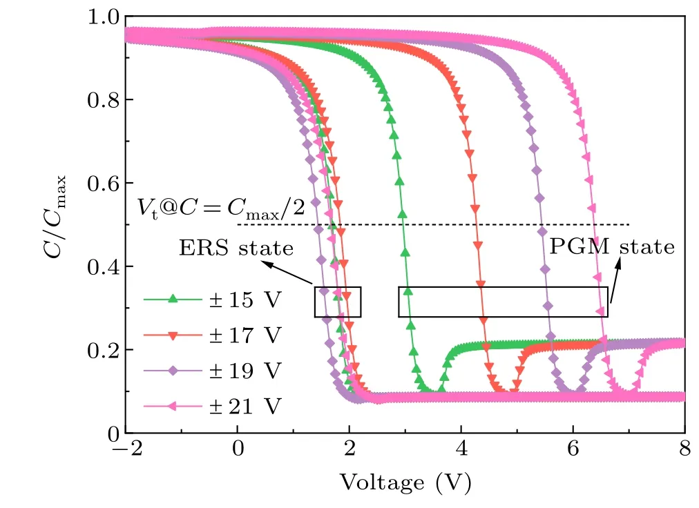
Fig.2.The C–V curves of an unirradiated CTM capacitor with different sweeping gate voltage ranges.
Figure 3 shows the normalizedC–Vcurves of CTM capacitors in the initial state after exposure to different ion fluences.TheC–Vcurves shift toward the negative direction in Fig.3,which suggests the net positive charges increased.The values of flat-band voltage (VFB) and mid-gap voltage (Vmg)for different ion fluence were extracted from Fig.3.The variation of net interface charge (ΔNit) and net oxide trap charge(ΔNot)in the trapping layer can be calculated by the following formula:[25,26]
where ΔVFBand ΔVmgare the difference ofVFBandVmgbefore and after irradiation,Coxis the oxide capacitance measured in accumulation,qis the electron charge (1.6×10⁻¹⁹C) andAis the gate electrode area(3.14×104μm2).
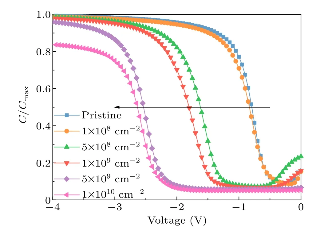
Fig.3.The C–V curves of CTM capacitors in the initial state at different ion fluences.
Figure 4 shows theVFB,Vmg, ΔNitand ΔNotchanging as a function of ion fluence.It can be seen that ΔNotincreases under irradiation, whereas ΔNitshows no obvious difference before and after irradiation.Therefore, this indicates that irradiation has a greater effect on bulk oxide than on the interface in CTM capacitors.In order to analyze the mechanism of the ion-induced variation of ΔNitand ΔNot, we calculated the vacancy density introduced by heavy ion irradiation using a SRIM model.The deduced vacancy density generated by ion irradiation is about 2.5×1018cm-3at the largest fluence of 1×10¹⁰ions/cm2, which is less than the intrinsic vacancy density in the trapping layer (about 1019cm-3[27,28]).It can be concluded that the positively charged vacancies induced by ion irradiation in the trapping layer are not the main reason for the increase of net positive charges.Thus, the increase of net positive charges in the oxide can be explained by the trapping effects of holes.In the initial state of a CTM capacitor,almost all charge traps in the trapping layer are empty.Heavy ions generate electron–hole pairs along their trajectory.Some electron–hole pairs recombine and others move in capacitors.The mobility of electrons is higher than that of holes, so the electrons are quickly ejected from the trapping layer,whereas the holes are captured in the trapping layer during transport.The accumulation of holes in the trapping layer causes the increase of net positive charges in the oxide.With the reduction of hole traps,ΔNotgradually saturates due to the limited number of intrinsic hole traps in the trapping layer.The decrease of ΔNotat a fluence of 1×10¹⁰ions/cm2is attributed to the degradation of the dielectric properties of the oxide layer induced by irradiation;[29]as shown in Fig.3,the capacitance in the accumulation region of the CTM capacitor decreased after irradiation with up to 1×10¹⁰ions/cm2.

Fig.4.(a) The VFB and Vmg as a function of ion fluence.(b) ΔNit and ΔNot of the CTM at different ion fluences.
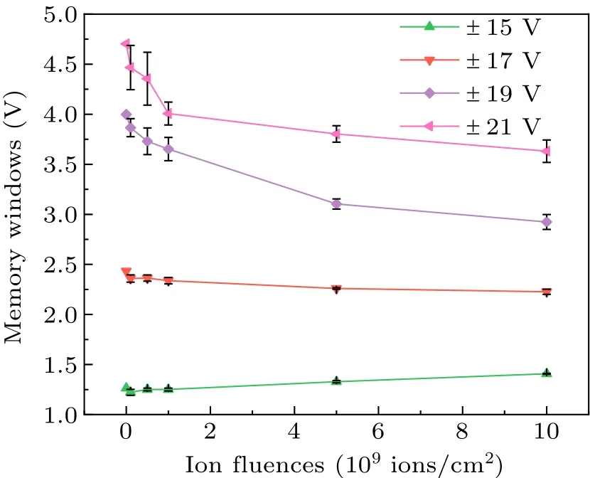
Fig.5.The relationship between memory window and ion fluence at different sweeping voltages.
The memory characteristics of the CTM capacitors are usually characterized by the memory window.Figure 5 shows the relationship between memory window and ion fluence at different sweeping voltages.When the sweeping voltage is low,the memory window is still small and independent of ion fluence.As the sweeping voltage is changed from±17 V to±21 V(high voltage),the memory window decreases with the increase in ion fluence.With the increase in applied voltage,the degradation trend of the memory window becomes more and more obvious.
In order to determine the factors affecting the memory window of the CTM capacitor, we analyzed the process of memory window formation with the help of the energy band diagram.Figure 6 illustrates the schematic energy band diagrams of the TiN/Al2O3/HfO2/Al2O3/HfO2/SiO2/p-Si structure in the program process.In the program process,a positive voltage is supplied to the top electrode.Many electrons tunnel through the tunneling layer into the trapping layer(defined asJe1in Fig.6).There are many intrinsic bulk traps and interface states in the trapping layer.The electrons in the trapping layer are trapped to complete the charge storage process(defined asJe2in Fig.6).Because the blocking layer is very thick,only a few electrons in the trapping layer tunnel through the blocking layer into the TiN gate (defined asJe3in Fig.6).The erase process is the converse.A negative bias is applied to the electrode and the erase process is completed by injecting holes into the trapping layer.The difference ofVtbetween these two processes is defined as the memory window which characterizes the charge trapping capability of the capacitor.Through the above analysis,it was found that the memory windows of CTM capacitors were mainly affected by the charge trap process(Je2process)and the charge loss process(Je3process)in the program process.

Fig.6.Energy band diagram of TiN/Al2O3/HfO2/Al2O3/HfO2/SiO2/p-Si memory structure in the program process.
The damage induced by irradiation in the tunneling layer and trapping layer does not contribute much to the change in the memory window.The tunneling layer is used to help facilitate electron tunneling in the program process at high voltage.The structural damage in the tunneling layer has negligible influence on the reduction of the memory window after irradiation.Besides, the deduced number of vacancies induced by irradiation in the trapping layer is very small compared to the number of intrinsic traps.It means that theJe2process of CTM capacitors has very little impact on the variation of the memory window.We suggest that the irradiationinduced structural damage in the blocking layer is the main reason for the reduction of the memory window.On the one hand, the defects in the blocking layer induced by irradiation become the auxiliary tunneling centers of electrons.The auxiliary tunneling centers lead to the discharge of the trapping layer.This process is called trap-assisted tunneling(TAT).[30]The TAT process enhances the charge loss process (Je3process in Fig.6).The probability of charge stored in the trapping layer tunneling out through the TAT process is related to the defect concentration[31–34]and supply voltage.[35,36]The larger the defect concentration,the higher the supply voltage,and the more influential theJe3process is.On the other hand,it was reported that ion latent tracks induced by heavy ion irradiation can induce the degradation of blocking layers and increase leakage current.[37–41]The (dE/dx)eof Ta ions is about 32.8 keV/nm in Al2O3, which exceeds the threshold value to form the latent tracks (6 keV/nm–10 keV/nm[42,43]).Thus,Ta ions can generate a localized region of physical damage (latent track) in the blocking layer, which enhances theJe3process.The capacitance in the accumulation region of the CTM capacitor decreased after being irradiated with up to 1×10¹⁰ions/cm2which means the dielectric constant of the oxide layer decreases with the irradiation fluence.[29]It was reported that the degradation of dielectric properties is due to structural damage of the oxide, thus it was proved that the structural damage induced by heavy ions does occur in the oxide dielectrics.
In summary,heavy ion irradiation has two effects.Firstly,heavy ions have a strong ionization ability.Heavy ions can ionize a large number of electron–hole pairs during irradiation.Secondly, heavy ions deposit a large amount of energy and generate high temperatures along their trajectories,which cause permanent structural damage within the material.The degradation of CTM capacitors caused by heavy ion irradiation is mainly reflected in two aspects: the threshold voltage shifts to the negative direction after irradiation and the memory window of the irradiated capacitors decreases with the increase of ion fluence.The negative shift of threshold voltage is due to the influence of the ionization process of heavy ions.Threshold voltage shifts caused by oxide trap charges can be recovered by program–erase operations.The decrease of the memory window is due to the structural damage induced by heavy ion irradiation in the blocking layer (Al2O3).The impact of the structural damage induced by heavy ion irradiation is permanent which cannot be recovered by other operations.In aerospace applications,more attention should be paid to the impact of permanent damage caused by heavy ion irradiation.
4.Conclusion
The effects of heavy ion irradiation on CTM capacitors have been investigated in this paper.It was observed that theC–Vcurves shifted toward the negative direction after heavy ion irradiation, which is due to the increase of net positive charges in the trapping layer.The effects of irradiation on interface charges and oxide trap charges were analyzed in detail.Combined with SRIM simulation, the contribution of defects introduced by irradiation into the trapping layer to the threshold voltage shift was quantitatively analyzed.We believe that the threshold voltage shift is caused by the accumulation of holes.Furthermore, the memory window of CTM capacitors decreased with an increase in ion fluence and the degradation of storage characteristics was more serious at high voltage,which result from an enhanced charge loss process due to the formation of defects and latent tracks in the blocking layer.This work is helpful to understand the mechanism of CTM performance degradation induced by heavy ion irradiation.
Acknowledgments
Project supported by the National Natural Science Foundation of China (Grant Nos.12105340, 12035019, and 12075290) and the Youth Innovation Promotion Association of the Chinese Academy of Sciences (Grant No.2020412).We would like to thank all the accelerator staff at the HIRFL accelerator.
猜你喜欢
Chinese Physics B(2022年11期)2022-11-21
Chinese Physics B(2022年9期)2022-09-24
Chinese Physics B(2022年5期)2022-05-16
杂文月刊(2019年18期)2019-12-04
21世纪(2019年10期)2019-11-02
21世纪(2019年10期)2019-11-02
21世纪(2019年9期)2019-10-12
美与时代·美术学刊(2018年10期)2018-01-25
汉语世界(2017年5期)2017-09-21
- Chinese Physics B的其它文章
- Dynamic responses of an energy harvesting system based on piezoelectric and electromagnetic mechanisms under colored noise
- Intervention against information diffusion in static and temporal coupling networks
- Turing pattern selection for a plant–wrack model with cross-diffusion
- Quantum correlation enhanced bound of the information exclusion principle
- Floquet dynamical quantum phase transitions in transverse XY spin chains under periodic kickings
- Generalized uncertainty principle from long-range kernel effects:The case of the Hawking black hole temperature