
Characterization of the N-polar GaN film grown on C-plane sapphire and misoriented C-plane sapphire substrates by MOCVD
2022-03-12 07:44XiaotaoHu胡小涛YimengSong宋祎萌ZhaoleSu苏兆乐HaiqiangJia贾海强WenxinWang王文新YangJiang江洋YangfengLi李阳锋andHongChen陈弘
Chinese Physics B 2022年3期
Xiaotao Hu(胡小涛) Yimeng Song(宋祎萌) Zhaole Su(苏兆乐) Haiqiang Jia(贾海强)Wenxin Wang(王文新) Yang Jiang(江洋) Yangfeng Li(李阳锋) and Hong Chen(陈弘)
1Key Laboratory for Renewable Energy,Beijing Key Laboratory for New Energy Materials and Devices,Beijing National Laboratory for Condensed Matter Physics,Institute of Physics,Chinese Academy of Sciences,Beijing 100190,China
2School of Physical Sciences,University of Chinese Academy of Sciences,Beijing 100049,China
3Songshan Lake Materials Laboratory,Dongguan 523808,China
4School of Mathematics and Physics,Beijing Key Laboratory for Magneto-Photoelectrical Composite and Interface Science,
University of Science and Technology Beijing,Beijing 100083,China
5College of Materials Science and Opto-Electronic Technology,University of Chinese Academy of Sciences,Beijing 100049,China
Keywords: metal-organic chemical vapor deposition(MOCVD),misoriented sapphire substrate,misorientation angle,x-ray diffraction,N-polar GaN
1. Introduction
Gallium nitride (GaN) is a fundamental semiconductor material that has been applied to light emitting diodes(LEDs),[1]laser diodes (LDs),[2]as well as high electron mobility transistors (HEMTs),[3]etc. Normally, GaN has a crystal structure of wurtzite, with C-plane (0001) as basal plane. Meanwhile, C-plane is a polar plane and it can exhibit two kinds of polarities, the Ga-polar (0001) and the Npolar (000¯1). The Ga-polar is the common polarity, and the Ga-polar GaN film can be grown by the metal-organic chemical vapor deposition (MOCVD) or the molecular beam epitaxy (MBE) on the sapphire (0001), Si (111), or the SiC substrates.[4-11]And the growth and the application of Gapolar GaN have been studied extensively and deeply.[6,11-17]On the other hand,the N-polar is the rare polarity,and the Npolar GaN film has many advantages over the Ga-polar GaN film. For example, in the N-polar AlGaN/GaN HEMT, GaN channel layer is on the top of AlGaN barrier layer. Such structure leads to lower resistance of Ohmic contact and less electron scattering in the channel compared with the Ga-polar Al-GaN/GaN HEMT. Besides, the N-polar GaN is easier to be manufactured into the enhancement mode transistors and the N-polar HEMTs have the advantage over Ga-polar HEMTs when they are scaled down.[18]Nevertheless, a high density of hexagonal hillocks appeared on the surface of the N-polar GaN layer grown on the C-plane sapphire by MOCVD.[19]The N-polar GaN without the hexagonal hillocks on the surface was grown by Matsuokaet al.[20]on the C-plane sapphire by MOCVD and it showed the surface and a small full width at half maximum(FWHM)of the x-ray rocking curves for the(000¯2)reflection. Kelleret al.[21]also grew the N-polar GaN without the hexagonal hillocks by MOCVD on the misoriented sapphire substrate,for the possible mechanism that the misoriented sapphire offered more steps and kinks that can promote the step flow growth. Nowadays, the crystalline quality and surface morphology of the N-polar GaN have been greatly improved, but the growth window is narrower than that of the Ga-polar GaN,because the growth mechanism,the crystal defects and the microstructure of the N-polar GaN are still lack of deep understanding.
X-ray diffraction (XRD) is an important tool in characterizing the thin film. The diffraction curves can be fitted by the Gaussian distribution function or the Lorentzian distribution function or more complex functions, like the Voigt,[22]the pseudo-Voigt[23]and the Pearson,[24]and these complex functions can approach the curve closer than the Gaussian function or Lorentzian function.[22]The mathematic form of the pseudo-Voigt function is a linear combination of Gaussian function and Lorentzian function,[24]and it is simpler than the form of the other two complex functions, so in this study we pick it as the fitting function. It is known[23,25]that in theω-2θscan for XRD,the Gaussian distribution function is only related to the vertical lattice-strain in the film,and the Lorentzian distribution function is only related to the vertical coherence length in the film. And in theωscan for XRD,the Gaussian function is only related to the tilt angle of crystallites in the film and the Lorentzian function is only related to the lateral coherence length in the film. Therefore, the contributions of the vertical lattice-strain and the vertical coherence length to the diffraction curve can be separated and the values of these two parameters can be calculated. Similarly,the tilt angle and the lateral coherence length can be calculated.
In this paper, the N-polar GaN film was grown on the C-plane sapphire and misoriented C-plane sapphire substrates respectively by MOCVD. The polarity of the film was testified and the morphology was studied. More importantly, the contributions of the vertical lattice-strain and the vertical coherence length and the contributions of the tilt angle and the lateral coherence length to the diffraction curve were separated respectively, and the influence of different misorientation angles on these parameters was investigated.
2. Experiment
The N-polar GaN film was grown on three sapphire substrates in one run by the AIXTRON G3[26]2400HT MOCVD.The three substrates were C-plane sapphire,C-plane sapphire with 2°off-axis toward M-plane,and C-plane sapphire with 4°off-axis toward M-plane.All the substrates were two inches in diameter and 430-μm-thick. The precursors were trimethylgallium (TMGa), trimethyl-aluminum (TMAl) and ammonia(NH3). The growth consisted of four steps. Firstly, the three substrates were kept at 1000°C for 20 min in an atmosphere of H2to desorb molecules on the surface. Next,a 3-min nitridation occurred at 1000°C in an atmosphere of NH3. Then,a 100-nm-thick AlN nucleation layer was grown. Lastly, the N-polar GaN layer was grown at 1050°C.The nominal thickness of the N-polar GaN layer was 1 μm. The reactor pressure was kept constant at 50 mbar during the growth. The three as-grown samples were named as sample 0M,sample 2M,and sample 4M,where 0M,2M and 4M represent the N-polar GaN film grown on the C-plane sapphire, on the C-plane sapphire with 2°off-axis toward M-plane and on the C-plane sapphire with 4°off-axis toward M-plane,respectively. To confirm the polarity of the as-grown films, we adopt the method of wet etching. The samples were first immersed in potassium hydroxide (KOH) solution (6 mol/L) at room temperature for 5 min, and then were observed under the scanning electron microscope(SEM,SIRION FP6800/73).
The XRD curves were recorded by the x-ray diffractometer(Malvern Panalytical EMPYREAN),using a wavelength of 1.540598 °A(CuKα1). The reflection geometry includes a Ge(220)hybrid monochromator and a hybrid pixel detector(PIXcel 3D).The surface morphology of the as-grown samples was examined by the optical microscope (OM, Nikon ECLIPSE LV15ON)and atomic force microscope(AFM,Bruker Multi-Mode 8,in ScanAsyst Mode).
To acquire the lateral coherence length and the tilt angle (the “lateral” means the direction is parallel to the surface of the film),we used the pseudo-Voigt function to fit the measured(000¯2)ω-scan curve,and the pseudo-Voigt function is[23]
P(x)=I0[ηL(x)+(1-η)G(x)],0 ≤η≤1,(1)whereL(x) andG(x) are the Lorentzian distribution function and the Gaussian distribution function, respectively,ηis the variable of the pseudo-Voigt function,andI0is a scaling constant. The lateral coherence length and the tilt angle were calculated using the following empirical formulae:[23]
whereλis the x-ray wavelength,θis the Bragg angle for the(000¯2) reflection, andβωis the integral breadth of the fitting curve.
To acquire the vertical coherence length and the vertical lattice-strain (the “vertical” means the direction is normal to the surface of the film),we used the pseudo-Voigt function to fit the (000¯2)ω-2θscan curve. And the vertical coherence length and the vertical lattice-strain were calculated using the following empirical formulae,respectively:[23]
whereβ2θ-θis the integral breadth of the fitting curve,andθis the Bragg angle for the(000¯2)reflection.
3. Results and discussion
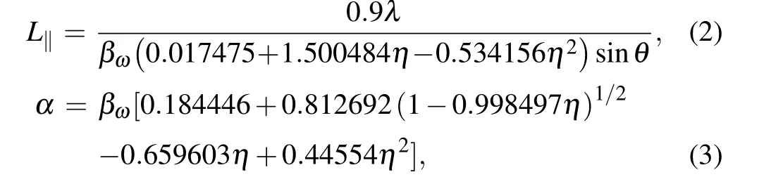
Figure 1 shows the SEM photographs of the samples before and after KOH etching. Before the etching, a hexagonal hillock is on the surface of sample 0M. After the etching, a hexagonal hillock can still be seen and many little hillocks appear on the surface, as shown in Figs. 1(a) and 1(b). These small hillocks are hexagonal too(the relevant photographs are given in Appendix A).As shown in Figs.1(c)and 1(d),before the etching,an irregular hexagonal hillock is on the surface of sample 2M, and many small hillocks also appear on the surface after the etching. Figure 1(e)shows the surface of sample 4M before KOH etching and some tortuous wrinkles can be seen on the surface. After KOH etching,as shown in Fig.1(f),the wrinkles are gone,and the surface is covered with many little hillocks. According to Ng, Weimann and Chowdhury,[27]Ga-polar GaN film remained intact in the KOH solution while N-polar film was etched in the solution and later on the surface was covered with many nanotip pyramids, which are consistent with the small hillocks in Figs.1(b),1(d),and 1(f).Therefore,it is confirmed that the three samples are all N-polar GaN thin films.
Fig.1. Plane-view SEM photographs of the as-grown samples((a),(c),(e))and the samples after KOH etching((b),(d),(f)). (a),(b)sample 0M;(c),(d)sample 2M;and(e),(f)sample 4M.The accelerate voltage,the spot size,and the magnification are all the same for these photographs.
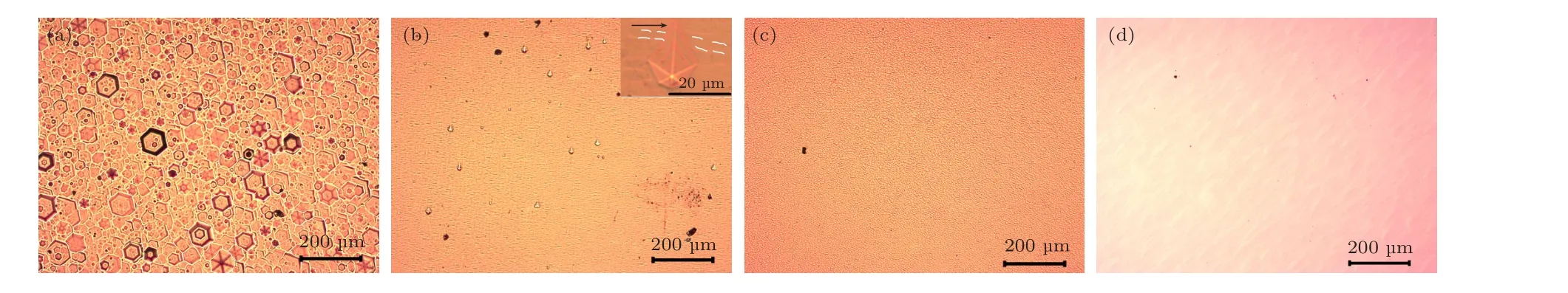
Fig.2. The plane-view optical micrographs of(a)-(d)samples 0M,2M,4M and a Ga-polar sample,respectively.
Figure 2 shows the photographs of the surface of N-polar GaN samples and a Ga-polar GaN sample taken by the optical microscope. Many hexagonal hillocks are on the surface of sample 0M,as shown in Fig.2(a). In Fig.2(b),a small number of hillocks are on the surface of sample 2M,and their sizes are smaller than those on the surface of sample 0M.An insert in Fig.2(b)shows an enlarged hillock,and we can see that the shape of the hillock is an irregular hexagon. The wrinkles on the surface,which are indicated by two broken white lines,can be clearly recognized. The sharpest corner in the insert indicated by a black arrow represents the fastest growth direction of the hillock,and this corner is perpendicular to the wrinkles on the surface. No hillocks appear on the surface of sample 4M, as shown in Fig. 2(c), and the surface is very smooth.Kelleret al.[21]have reported similar results. What’s more,our results show that the shape of the hillocks on sample 2M is irregular and all the hillocks’sharpest corner is parallel to the misorientation direction of the sapphire substrate. We believe that the irregular shape of the hexagonal hillocks is caused by the misoriented substrate. From sample 2M to 4M,the density of hillocks can drop to zero. The explanation is that increasing the misorientation angle leads to the increase of the step density on the surface of the sapphire substrate, and adatoms can combine with each other more easily because of the decreased distance between adjacent steps. Therefore, they are more likely to coalesce into one complete film. Finally, the Ga-polar GaN sample exhibits a smooth surface,as shown in Fig. 2(d), and this sample is grown on the C-plane sapphire substrate. The difference of Ga-polar and N-polar GaN is that it is easy to get Ga-polar GaN film with a smooth surface on C-plane sapphire substrate, while smooth N-polar GaN film can only appear on misoriented substrate with a proper misorientation angle.
The root-mean-square roughness of samples 0M,2M and 4M is 5.19 nm, 2.64 nm and 5.26 nm, respectively. Of the three samples,sample 2M has the lowest roughness. And the morphology of samples 2M and 4M is different from that of sample 0M.As shown in Figs.3(b)and 3(c),small undulations with peaks and valleys[21]can be clearly seen on the surfaces of samples 2M and 4M,while a hillock-like morphology can be seen on the surface of sample 0M in Fig.3(a). The undulations of samples 2M and 4M are probably due to the step bunching.[21]In general,the morphology of the N-polar GaN changes from hillocks on the C-plane sapphire to the undulations with peaks and valleys on the misoriented sapphire.
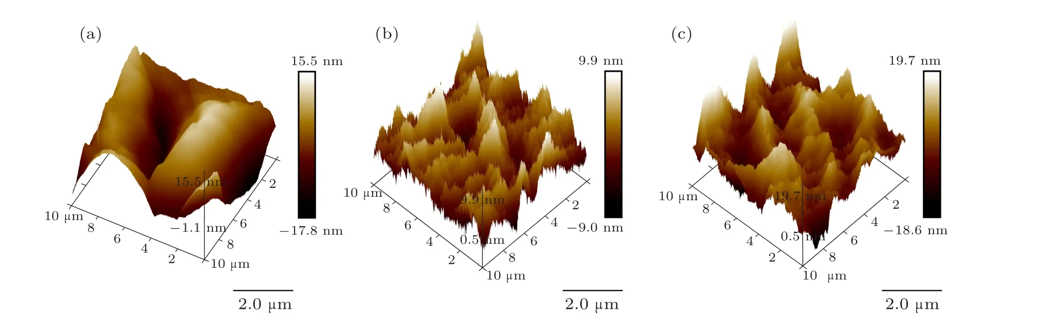
Fig.3. (a)-(c)The AFM images of the surfaces of samples 0M,2M and 4M,respectively. The scanning area is 10×10 μm2.
Figure 4 shows the FWHM of (000¯2) and (10¯1¯2) of the samples for the x-ray rocking curves. With the increase of the substrate misorientation angle,the FWHM of(10¯1¯2)is greatly improved (from 770 arcsec to 450 arcsec), while the FWHM of (000¯2) shows a modest increase especially when the misorientation angle is not too large. The result implies that further increase of the misorientation angle of the sapphire substrate probably leads to the deterioration of crystal quality of the GaN film. In general,the crystalline quality of the N-polar GaN film is improved by introducing the substrate misorientation.
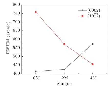
Fig.4. The FWHM of(000¯2)and(10¯1¯2)of the three samples for the x-ray rocking curves,with the symbol squares and circles representing the FWHM of(000¯2)and(10¯1¯2),respectively.
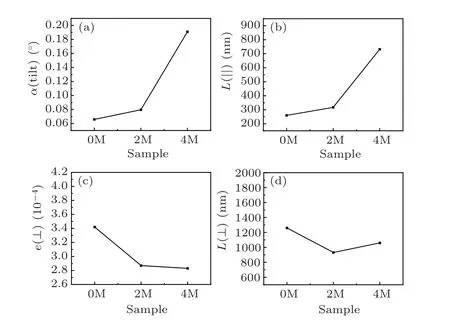
Fig. 5. The calculated (a) tilt angle, (b) lateral coherence length, (c) vertical lattice-strain,(d)vertical coherence length of the three samples from the pseudo-Voigt function fit.
As shown in Fig. 5(a), from sample 0M to 2M and then to 4M,the tilt angle increases. This means that the crystallites deviate more from the[000¯1]orientation when growing on the misoriented substrate,so the crystal orientation of the N-polar GaN film is degraded. This situation gets worse when the misorientation angle increases. The lateral coherence length increases too,as shown in Fig.5(b). The explanation is that the substrate of sample 4M contains higher density of steps on the surface than those of 2M and 0M do. During the growth, the adatoms at the steps of sample 4M’s surface only need to diffuse a short distance to the adjacent step to combine with other adatoms to form a crystallite, and hence the crystallites have larger lateral length.As shown in Fig.5(c),from sample 0M to 2M and then to 4M,the vertical lattice-strain decreases. Furthermore,from sample 0M to 2M,the decrease of the latticestrain is significant,while from sample 2M to 4M,it is much less. It means that the misorientation angle has limited effect on the decrease of the vertical lattice-strain. The vertical coherence lengths of samples 0M,2M and 4M do not show much difference,as shown in Fig.5(d),and the lengths of the three samples are all close to 1 μm,which is the nominal thickness of the samples,and this result is similar to that of the Ga-polar GaN film.[23]
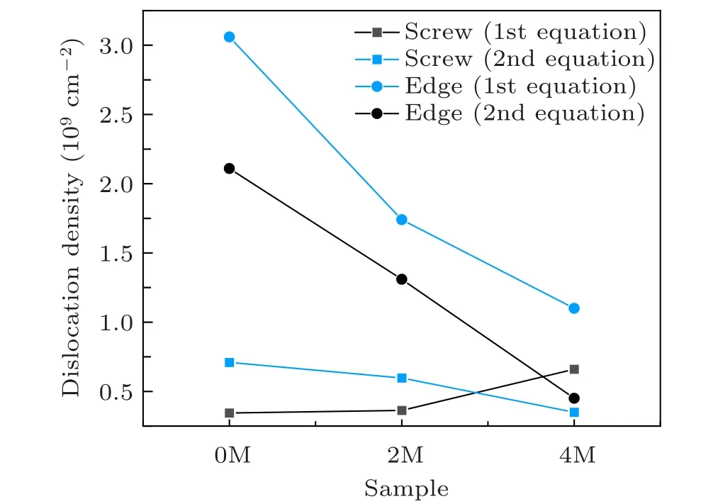
Fig. 6. The calculated screw and edge dislocation density of samples 0M,2M and 4M.
It is known that the FWHM of(000¯2)of XRD can be used to calculate the density of the screw threading dislocations(b=〈0001〉,|b|=0.5185 nm), and the FWHM of (10¯1¯2) of XRD can be used to calculate the density of the edge threading dislocations(b=1/3〈11¯20〉,|b|=0.3189 nm).[21]The dislocation density is overestimated because the mixed dislocation(b=1/3〈11¯23〉)can contribute to FWHM of both reflections.To calculate the density of dislocation, we use two different equations. The first one isN=β2/(4.35·b2),and the second one isN=β/(2.1·b·d0),βis the FWHM of the x-ray rocking curves,bis the magnitude of the burgers vector,andd0in the second equation is the spacing between subgrain boundary according to Dunn and Koch.[28]The difference between the two equations is that the first one assumes that the dislocations are randomly distributed in the film,while the second assumes that the dislocations only locate at the boundary of subgrains.In this case, we can consider the mosaic blocks as the subgrains and use the lateral coherence length to replace thed0.The results are given in Fig. 6. An interesting phenomenon can be seen, that is, the screw dislocation density of sample 4M calculated from the first equation is the largest among the three samples,while from the second equation it is the smallest. On the contrary, the screw dislocation density of sample 0M calculated from the first equation is the smallest, while from the second equation it is the largest. The edge dislocation density of each sample calculated from the first equation is larger than that calculated from the second equation.
4. Conclusion
The N-polar GaN films were grown on the C-plane sapphire substrate, the C-plane sapphire with 2°off-axis toward M-plane and the C-plane sapphire with 4°off-axis toward Mplane by MOCVD.The polarity was testified by the KOH solution etching and the SEM observation. The density of the hexagonal hillocks on the surface of the samples drops as the misorientation angle increases.The crystalline quality of samples 2M and 4M is better than that of sample 0M, and sample 2M has lower RMS roughness than samples 0M and 4M.However, a small density of irregular hexagonal hillocks still appears on the surface of sample 2M,which is a problem that needs to fix in the future. The increase of the misorientation angle can enlarge the tilt angle and the lateral coherence length of the crystallites. What’s more, the increase of the misorientation angle can lower the vertical lattice-strain, but do not influence much on the vertical coherence length. This study helps to understand the influence of the misorientation angle of the misoriented C-plane sapphire on the morphology, the crystalline quality and the microstructure of the N-polar GaN film.
Acknowledgements
This work was supported by the National Natural Science Foundation of China(Grant No.61991441),the Strategic Priority Research Program of Chinese Academy of Sciences(Grant No. XDB33000000), and Youth Innovation Promotion Association of Chinese Academy of Sciences. We thank Yang X A from the Advanced Materials Laboratory, Institute of Physics,Chinese Academy of Sciences,for the experimental work of scanning electron microscope(SEM Sirion).

- Chinese Physics B的其它文章
- Measurements of the 107Ag neutron capture cross sections with pulse height weighting technique at the CSNS Back-n facility
- Measuring Loschmidt echo via Floquet engineering in superconducting circuits
- Electronic structure and spin-orbit coupling in ternary transition metal chalcogenides Cu2TlX2(X =Se,Te)
- Review on typical applications and computational optimizations based on semiclassical methods in strong-field physics
- Quantum partial least squares regression algorithm for multiple correlation problem
- Optical scheme to demonstrate state-independent quantum contextuality