
Improved thermal property of strained InGaAlAs/AlGaAs quantum wells for 808-nm vertical cavity surface emitting lasers
2022-03-12 07:48ZhuangZhuangZhao赵壮壮MengXun荀孟GuanZhongPan潘冠中YunSun孙昀JingTaoZhou周静涛andDeXinWu吴德馨
Chinese Physics B 2022年3期
Zhuang-Zhuang Zhao(赵壮壮), Meng Xun(荀孟), Guan-Zhong Pan(潘冠中),Yun Sun(孙昀), Jing-Tao Zhou(周静涛), and De-Xin Wu(吴德馨)
Institute of Microelectronics,Chinese Academy of Sciences,Beijing 100029,China
Keywords: 808-nm VCSEL,InGaAlAs/AlGaAs quantum wells,thermal property
1. Introduction
Vertical cavity surface emitting lasers (VCSELs) have significant advantages such as circular output beams, low threshold currents, single longitudinal modes, high speed modulations, slow wavelength shift ratesversustemperature,and easy two-dimensional integrations.[1-6]The VCSELs have been widely used in data communication and short-distance optical interconnection.[7-11]In recent years, the VCSELs have been greatly developed and widely used in the fields of three-dimensional face recognition,hand gesture recognition,and laser radar.[12]
The wavelength of 808 nm is a very important wavelength in high-power laser applications. For example, the 808-nm laser source can be used as a pump source of solidstate laser (Nd:YAG or Nd:YVO4) used for material cutting,marking,printing,etc.[13-15]The 808-nm pulsed laser sources are also used in the medical field for skin-care related cosmetic applications such as hair removal,[16]and they also used as industrial and military infra-red illumination sources.[17,18]Compared with the conventional 808-nm edge-emitting semiconductor lasers,VCSELs have good wavelength stability for varying environment temperatures. The VCSELs also exhibit a small divergence angle and circular output beam, which is conducive to the collimation or focusing.
To date, there have been not many reports on 808-nm VCSELs. These reports focused mainly on how to solve the heat dissipation problem in order to increase the output power in practical applications. Because of strong GaAs absorption at 808 nm, a bottom-emitting configuration cannot be used for efficient heat dissipations. Seurinet al.demonstrated 3 mm×3 mm arrays and 5 mm×5 mm arrays with the GaAs substrate completely removed from and mounted on diamond submounts. These arrays emit more than 50 W and 120 W,respectively, and exhibit a maximum power conversion efficiency of 42%.[19]Zhonget al.improved thermal stability of 808-nm VCSEL arrays by arranging the mesa distribution within the array in a nonlinear configuration.[20]Besides exploring heat dissipation measurement, it is also important to reduce the self-heating of the device for improving the temperature stability of the device. In VCSELs,the quantum well material is critical for differential gain and temperature stability. Zhanget al.numerically simulated GaAs/Al0.3Ga0.7As,GaAsxP1-x/Al0.3Ga0.7As and In1-x-yGaxAlyAs/Al0.3Ga0.7As quantum-well active regions. The output characteristics of the three designed quantum-well VCSELs were also calculated and compared.[21]
In this work, we design and fabricate two kinds of 808-nm VCSELs with In0.13Ga0.75Al0.12As/Al0.3Ga0.7As and Al0.05Ga0.95As/Al0.3Ga0.7As quantum wells,respectively.The temperature characteristics of the two kinds of quantum wells are investigated mainly by theory. Then the output power characteristics and temperature characteristics of the fabricated VCSELs are analyzed in detail. The strained In0.13Ga0.75Al0.12As/Al0.3Ga0.7As quantum wells exhibit higher material gain and better temperature stability than Al0.05Ga0.95As/Al0.3Ga0.7As quantum wells. The tested results are in good agreement with the calculations. The VCSELs with strained InAlGaAs quantum wells are more suitable for high temperature operation.
2. Design and fabrication
The 808-nm top emitting laser layers to be examined here were grown by metal-organic chemical vapor deposition (MOCVD) on an N-type GaAs substrate. The bottom mirror consisted of 41.5 pairs of Ndoped Al0.25Ga0.75As/Al0.9Ga0.1As distributed Bragg reflectors (DBRs). The top mirror was composed of 23.5 pairs of P-doped Al0.25Ga0.75As/Al0.9Ga0.1As DBRs. The active region contained three pairs of 6-nm-thick In0.13Ga0.75Al0.12As quantum wells surrounded by 8-nm-thick Al0.3Ga0.7As barrier layers. Another kind of active region containing three pairs of 6-nm-thick Al0.05Ga0.95As quantum wells surrounded by 8-nm-thick Al0.3Ga0.7As barrier layers was also designed for contrast.
The fabrication procedure is as follows. Firstly,Ti/Pt/Au electrode was deposited at the periphery of output aperture.The P-DBRs were etched by inductively coupled plasma(ICP)reactive ion etching to expose the Al0.98Ga0.02As layer. The oxide aperture was formed by the selective wet oxidation of Al0.98Ga0.02As into AlxOyat temperature of 420°C. A 200-nm-thick SiN layer was deposited on the surface of the VCSEL for electric isolation. After Ti/Au seed layer was sputtered, thick Au is electroplated to improve heat dissipation.Then,the substrate was thinned to 150 μm. The N-type electrode was evaporated on the substrate.Finally,the contacts are rapidly annealed in a nitrogen(N2)ambient.Figure 1(a)shows a microscopic image of the fabricated 808-nm VCSELs. Figure 1(b) shows the cross-section diagram of the 808-nm VCSEL along the A-A′direction in Fig.1(a).

Fig. 1. (a) Microscopic image of actual device, and (b) cross-section diagram of device along A-A′ direction.
3. Results and discussion
The gains of In0.13Ga0.75Al0.12As/Al0.3Ga0.7As and Al0.05Ga0.95As/Al0.3Ga0.7As quantum wells at different ambient temperatures are calculated by the standard 8-bandk· ptheory,[22]and the results are shown in Figs. 2(a)and 2(b). At the same ambient temperature, the gain of In0.13Ga0.75Al0.12As quantum wells is higher than that of Al0.05Ga0.95As quantum wells. This is because the strain of In0.13Ga0.75Al0.12As quantum wells increases the curvature of the valence band structure,thereby greatly reducing the effective mass. The strain can reduce the valence band effective mass allowing the quasi-Fermi levels to separate more symmetrically. So not only does the material turns transparent faster, but also the gain increases faster with carrier density increasing.[23,24]

Fig. 2. (a) Curves of gain versus wavelength of three pairs of 6-nmthick In0.13Ga0.75Al0.12As quantum wells surrounded by 8-nm-thick Al0.3Ga0.7As barrier layers at different temperatures, and (b) curves of gain versus wavelength of three pairs of 6-nm-thick Al0.05Ga0.95As quantum wells surrounded by 8-nm-thick Al0.3Ga0.7As barrier layers at different temperatures.
Owing to increased leakage carriers at high temperatures,the gains of these two kinds of quantum wells decrease as the ambient temperature increases. The variation of the extracted peak gain with ambient temperature is shown in Fig.3(a). The drop rate of Al0.05Ga0.95As quantum wells’peak gain decreasing with ambient temperature increasing is 19.18 cm-1/°C which is faster than that of In0.13Ga0.75Al0.12As quantum wells, 17.26 cm-1/°C. In addition, the gain curves of these two kinds of quantum wells are redshifted as the ambient temperature increases. The red shift rate of the peak wavelength of In0.13Ga0.75Al0.12As quantum wellsversustemperature increasing is 0.220 nm/°C which is slower than that of Al0.05Ga0.95As quantum wells, 0.275 nm/°C as indicated in Fig. 3(b). The above calculation results show that the In0.13Ga0.75Al0.12As quantum wells exhibit higher material gain and better high-temperature stability than Al0.05Ga0.95As quantum wells.
In addition, the gains of Al0.05Ga0.95As and In0.13Ga0.75Al0.12As quantum wells with 4 nm and 8 nm in widths are also calculated at different ambient temperatures as shown in Fig. 4. The barrier material is still Al0.3Ga0.7As with 8 nm in width. Obviously, the gains of the In0.13Ga0.75Al0.12As quantum wells with 4 nm and 8 nm in widths are significantly greater than those of the Al0.05Ga0.95As quantum wells at the same ambient temperature.This trend agrees with the result of 6-nm quantum well in Fig.2. From Figs.2 and 4,the difference in gain between the two quantum wells turns smaller as the well width increases from 4 nm to 8 nm at the same temperature. As the well width is 4 nm, 6 nm, and 8 nm, the corresponding gain difference between the In0.13Ga0.75Al0.12As and Al0.05Ga0.95As quantum wells is 2239.8 cm-1, 1418.9 cm-1, and 834.9 cm-1at temperature of 30°C.

Fig.3. Plots of(a)peak gain and(b)peak wavelength versus ambient temperature of Al0.05Ga0.95As and In0.13Ga0.75Al0.12As quantum wells with 6-nm width.

Fig.4. Plots of gain versus wavelength of Al0.05Ga0.95As quantum wells with(a)4-nm and(d)8-nm widths at different temperatures. Plots of gain versus wavelength of In0.13Ga0.75 Al0.12As quantum wells with(b)4-nm and(d)8-nm widths. Plots of peak gain versus ambient temperature of Al0.05Ga0.95As and In0.13Ga0.75 Al0.12As quantum wells with(c)4-nm and(f)8-nm widths.
When the quantum well width is 4 nm, the peak-gain-dropping rate with temperature increasing for In0.13Ga0.75Al0.12As quantum wells and Al0.05Ga0.95As quantum wells are 28.09 cm-1/°C and 28.66 cm-1/°C, respectively. When the quantum well width is 8 nm, the peak-gain-dropping rate of In0.13Ga0.75Al0.12As quantum wells and Al0.05Ga0.95As quantum wells are 13.38 cm-1/°C and 13.71 cm-1/°C,respectively. Therefore,the In0.13Ga0.75Al0.12As is surely more stable than Al0.05Ga0.95As quantum wells with the temperature varying. It is also found that the quantum well with larger width exhibits more stable temperature performance. However,the gain decreases as the quantum well width increases. Therefore,the 6-nm well width is very suitable in terms of both gain and temperature stabilities.
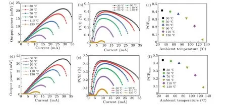
Fig.5. Plots of(a)output power,(b)PCE,and(c)maximum PCE versus current of the Al0.05Ga0.95As quantum wells VCSELs with 10-μm oxide aperture in a temperature range of 30 °C-130 °C,and plots of(d)output power,(e)PCE,and(f)maximum PCE versus ambient temperature of In0.13Ga0.75Al0.12As quantum wells VCSELs with 10-μm oxide aperture in a temperature range of 30 °C-130 °C.
The VCSELs with different oxide aperture diameters are fabricated and tested. TheL-Icharacteristics of the 10-μm VCSELs with both Al0.05Ga0.95As quantum wells and In0.13Ga0.75Al0.12As quantum wells at ambient temperatures ranging from 30°C to 130°C are shown in Figs. 5(a)and 5(b). It can be found that the output power of the In0.13Ga0.75Al0.12As quantum wells VCSELs is greater than that of the Al0.05Ga0.95As quantum wells VCSELs at the same ambient temperature and injection current.The maximum output power of In0.13Ga0.75Al0.12As quantum wells VCSELs is 22.88 mW at 30°C. As the ambient temperature increases,the output power gradually decreases. The maximum output power is 15.82 mW at 70°C and 1.52 mW at 130°C. The maximum power of Al0.05Ga0.95As quantum wells VCSELs is 21.37 mW at 30°C,13.35 mW at 70°C,and only 0.031 mW at 130°C. The output power of In0.13Ga0.75Al0.12As quantum wells VCSELs decreases more slowly with the increase of ambient temperature. Therefore, the In0.13Ga0.75Al0.12As quantum wells VCSELs exhibit better high-temperature performances than Al0.05Ga0.95As quantum wells VCSELs.
The power conversion efficiency (PCE) of the VCSELs with two kinds of quantum wells under different ambient temperatures are shown in Figs. 5(b) and 5(e). As the ambient temperature is 30°C, the maximum power conversion efficiency (PCE) of In0.13Ga0.75Al0.12As quantum wells VCSELs can reach 43.82% which is higher than that of Al.05Ga0.95As quantum wells VCSELs, 41.33%. As the ambient temperature increases to 130°C, the maximum PCE for In0.13Ga0.75Al0.12As quantum wells VCSELs and Al0.05Ga0.95As quantum wells VCSELs decrease to 8.35%and 3.36%, respectively. The plots of maximum PCE of the two devicesversusambient temperature are shown in Figs. 5(c)and 5(d). Obviously,the maximum PCE of the Al.05Ga0.95As quantum wells VCSELs decreases faster with the increase of ambient temperature. Under the same operation condition,the In0.13Ga0.75Al0.12As quantum wells VCSELs have higher output power and higher power conversion efficiency than the Al0.05Ga.95As quantum wells VCSELs, showing better hightemperature stability. The experimental results are consistent with the calculations.
Figure 6(a)shows the plots of peak output powerversusambient temperature of In0.13Ga0.75Al0.12As quantum wells VCSELs with six oxide aperture diameters in a range of 2 μm-25 μm. The peak output power of VCSELs with the same oxide aperture decreases almost linearly with ambient temperature increasing. The extracted drop rate of peak output power increasing with oxide aperture increasing is shown in Fig.6(b).The drop rate of the peak output power of the VCSELs with an oxide aperture diameter of 2 μm, 10 μm, and 25 μm are 0.0471 mW/°C, 0.1901 mW/°C, and 0.4996 mW/°C, respectively. This is because larger active region area produces more heat, which will introduce more serious heat crosstalk.The heat dissipation in large aperture VCSELs is more difficult than that in small aperture VCSELs. As the ambient temperature increases,the phenomenon turns more serious,which accelerates the temperature rise. Therefore,the small aperture VCSELs exhibit more stable temperature characteristics.

Fig.6. (a)Plots of peak output power versus ambient temperature of In0.13Ga0.75Al0.12As quantum wells VCSELs with 2-μm-25-μm oxide apertures,and(b)plot of drop rate of peak output power versus oxide aperture.

Fig.7.(a)Rollover current and(b)rollover current density versus ambient temperature of 808-nm In0.13Ga0.75Al0.12As quantum wells VCSELs with 2-μm-25-μm oxide apertures.
The rollover current of VCSELs with an oxide aperture diameter of 2 μm and 25 μm at 30°C are 9.4 mA and 69 mA,respectively. When the ambient temperature rises to 110°C,the rollover currents become 5 mA and 27.5 mA,respectively,as shown in Fig. 7(a). It is noted that VCSELs with a larger oxide aperture have higher rollover currents. As the ambient temperature increases,the rollover current of the VCSELs with large oxide aperture decreases more quickly than that of the VCSELs with small oxide aperture. Figure 7(b) shows that the plots of rollover current density of VCSELsversuscurrent density for different oxide apertures. The rollover current density of 2-μm and 25-μm VCSELs at 30°C are 299.21 kA/cm2and 14.06 kA/cm2, respectively. As the temperature increases to 110°C, the rollover current density decreases to 159.15 kA/cm2and 5.60 kA/cm2,respectively.It indicates that the rollover current density of VCSELs with larger oxide aperture is smaller.With the increase of ambient temperature, the rollover current density of the VCSELs with small oxide aperture decreases faster than that of the VCSELs with large oxide aperture.
The plots of the output power of the In0.13Ga0.75Al0.12As quantum wells VCSELsversusinjection current are shown in Fig.8(a). The changes of output power of VCSELs with different oxide apertures are basically the same under small injection currents. As the injection current increases, the output power of the VCSELs with small oxide aperture decreases faster because the VCSELs with small oxide aperture has a small rollover current. Figure 8(b) shows the change of the output power of the In0.13Ga0.75Al0.12As quantum wells VCSELs with injection current density as the ambient temperature increases from 30°C to 90°C. Under the same current density, the change of output power increases with the augment of the oxide aperture diameter. This is because the rollover current density of VCSELs with large oxide aperture is lower than that of VCSELs with small oxide aperture. Obviously,the VCSELs with small oxide aperture have more excellent high-temperature stability than large oxide aperture VCSELs.
To investigate the thermal characteristics of In0.13Ga0.75Al0.12As quantum wells VCSELs,the thermal resistance is also calculated according to the emission spectra and the dissipated power. Thermal resistance can be determined experimentally from the following equation:[25]
where Δλ/ΔPdissis calculated by the variation of the wavelength shift with the dissipated power. The dissipation power is calculated by the input power subtracting the output power. Figure 9(a) shows that the value of Δλ/ΔPdissof In0.13Ga0.75Al0.12As quantum wells VCSELs with 10-μm oxide aperture at 30°C, 50°C, 70°C, 90°C, and 110°C are 0.1325 nm/mW,0.1366 nm/mW,0.1434 nm/mW,0.1525 nm/mW, and 0.1615 nm/mW, respectively. Δλ/ΔThsis calculated by the peak wavelength shift rateversusambient temperature,and its value is 0.0602 nm/°. At the ambient temperatures of 30°C,50°C,70°C,90°C,and 110°C,the thermal resistances are 2.201 K/mW,2.269 K/mW,2.382 K/mW,2.533 K/mW, and 2.683 K/mW, respectively, as shown in Fig.9(b).

Fig.8. Plots of output power of In0.13Ga0.75Al0.12As quantum wells VCSELs versus(a)injection current and(b)injection current density as ambient temperature increases from 30 °C to 90 °C.

Fig. 9. (a) The Δλ/ΔPdiss of In0.13Ga0.75Al0.12As quantum wells VCSELs with 10-μm oxide aperture versus dissipated power at different ambient temperatures,and(b)Δλ/ΔThs and thermal resistance versus ambient temperature.
4. Conclusions
In conclusion, the theoretical calculations show that the strained In0.13Ga0.75Al0.12As/Al0.3Ga0.7As quantum wells possess higher material gain and lower temperature sensitivity than the Al0.05Ga0.95As/Al0.3Ga0.7As quantum wells. The 808-nm vertical cavity surface emitting lasers with various oxide apertures are fabricated and characterized in this paper. It is demonstrated that the vertical cavity surface emitting lasers with strained In0.13Ga0.75Al0.12As/Al0.3Ga0.7As quantum wells exhibit higher power conversion efficiency (PCE) and better temperature stability. Such the vertical cavity surface emitting laser of 808-nm In0.13Ga0.75Al0.12As/Al0.3Ga0.7As quantum wells will be preferred for high power applications.The maximum PCE of 43.8%for 10-μm VCSELs is achieved at the ambient temperature of 30°C. The output power and spectra of the VCSELs under different ambient temperatures are tested. We find that the smaller oxide aperture VCSELs exhibit more stable temperature performance. The thermal resistances at different temperatures are also presented.
Acknowledgements
Project supported by the National Natural Science Foundation of China (Grant No. 61804175), the Key Research Program of Frontier Sciences, Chinese Academy of Sciences(Grant No. ZDBS-LY-JSC031), and the China Postdoctoral Science Foundation(Grant No.BX20200358).
- Chinese Physics B的其它文章
- Measurements of the 107Ag neutron capture cross sections with pulse height weighting technique at the CSNS Back-n facility
- Measuring Loschmidt echo via Floquet engineering in superconducting circuits
- Electronic structure and spin-orbit coupling in ternary transition metal chalcogenides Cu2TlX2(X =Se,Te)
- Characterization of the N-polar GaN film grown on C-plane sapphire and misoriented C-plane sapphire substrates by MOCVD
- Review on typical applications and computational optimizations based on semiclassical methods in strong-field physics
- Quantum partial least squares regression algorithm for multiple correlation problem