
Independently tunable dual resonant dip refractive index sensor based on metal-insulator-metal waveguide with Q-shaped resonant cavity
2022-03-12 07:48HaowenChen陈颢文YunpingQi祁云平JinghuiDing丁京徽YujiaoYuan苑玉娇ZhentingTian田振廷andXiangxianWang王向贤
Chinese Physics B 2022年3期
Haowen Chen(陈颢文) Yunping Qi(祁云平) Jinghui Ding(丁京徽) Yujiao Yuan(苑玉娇)Zhenting Tian(田振廷) and Xiangxian Wang(王向贤)
1College of Physics and Electronic Engineering,Northwest Normal University,Lanzhou 730070,China
2School of Science,Lanzhou University of Technology,Lanzhou 730050,China
3Engineering Research Center of Gansu Province for Intelligent Information Technology and Application,Northwest Normal University,Lanzhou 730070,China
Keywords: surface plasmon polaritons, refractive index sensors, metal-insulator-metal (MIM) waveguide,multi-mode interference coupling theory
1. Introduction
Surface plasmon polariton (SPP) is a kind of evanescent wave, which is formed when electromagnetic waves interact with metal surface charges and then collectively oscillate and intensify in a small range.[1-5]It can break the diffraction limit of light and is highly sensitive to different metals, environments,nanoscale shapes and sizes. Metal-insulator-metal(MIM) waveguide is one of the excitation sources for SPPs.In recent years, MIM waveguides have received widespread attention due to their simple structure, small size and easy integration.[6-8]As time went by,various functional photonic devices such as filters,[9]sensors,[10,11]optical switches,[12]slow light devices[13]and splitters[14]designed based on MIM waveguide structures have made great breakthrough in theoretical research and experiments.
As one of the important optical components in many devices,[15-21]sensors have received extensive attention in the past decades. Sensitivity (S) is an important indicator to judge the performance of the sensor and higher sensitivity means higher detection range.[22]In the past few years,researchers have designed many representative sensors based on the MIM waveguide. Yanet al.proposed a MIM waveguide based annular resonator with a sensitivity of 921 nm/RIU in 2015.[23]Liet al.designed a dual circular cavity waveguide through type refractive index sensor with a sensitivity of 840 nm/RIU[24]and Tanget al.presented a MIM-coupled resonant cavity based on Fano resonant refractive index sensor with an enhanced sensitivity of 1125 nm/RIU in 2017.[25]However, the above mentioned results still have the problem of poor sensitivity as well as the impossibility of tuning each resonant mode separately.
In this work,a refractive index sensor with independently tunable dual resonant dip based on a MIM waveguide with Qshaped cavity is designed. The structure of the sensor mainly consists of a MIM waveguide coupled with Q-shaped resonant cavity. Firstly, the transmission properties of SPPs are investigated by finite difference time domain(FDTD)method.Secondly, the dispersion equation is used for explaining the excitation process of SPPs in the MIM waveguides. The transmission performance of the sensor is theoretically analyzed by using the multimode interference coupled mode theory(MICMT)and the theoretical results are highly matched with the simulation results. And then,the relationship between the sensitivity of the two resonant dips and the model parameters is investigated. Numerical simulations show that the movement of dip I is mainly influenced by the lengthLand widthwof the rectangular cavity. Similarly,by fixing the length and width of rectangular cavity, dip II will change when the radius of the annular cavity varies while dip I remains the same.Consequently, dips I and II can be tunable independently by adjusting the geometric parameters of rectangular cavity and the annular cavity. In the meantime,multiple resonant modes indicate that the increased parallel processing power and the independent control of resonant points imply a greater range of applications. At optimum parameter settings, the sensitivity and figure of merit(FOM)are up to 1578 nm/RIU and 175,respectively, and this exceeds the sensing performance of the most devices. Due to its subwavelength scale and simple configuration,the device is easy to fabricate and highly integrated with other nanoscale devices.
2. Device model and theoretical analysis
The 3D model of the structure designed in this paper is shown in Fig.1(a),where the yellow part is silicon(Si)and the blue part is silver(Ag),and the whole cavity is formed by etching. When the gap width of the waveguide is about 50 nm,the difference between the 3D model and the 2D model is about zero.[26]In addition, 2D simulation of MIM plasmonic system is used by most researchers for its ability to test devices performance with shorter simulation times and lower losses,and so does this work.[27]Figure 1(b)is the 2D model,where the white part is air and the blue part is silver (Ag), S1is the incident waveguide, and S2is the outgoing waveguide. The rectangular cavity is named as cavity 1 (C1) and the annular cavity is named as cavity 2(C2)(both C1 and C2 are used in the following text), C1 is at an angle of 45°from the horizontal. The geometric parameters of Fig. 1 are set to be as follows: waveguide widthd=50 nm, C1 widthw=60 nm and lengthL=200 nm,C2 radiusR=200 nm,circular cavity radiusr=120 nm,and baffle thicknessg=10 nm.

Fig.1. (a)The 3D schematic diagram of MIM waveguide coupled with the Q-shaped cavity.(b)The 2D schematic diagram of MIM waveguide coupled with the Q-shaped cavity.
It is all known that TM polarized light is used as the excitation source of the MIM waveguide.The boundary conditions of the TM polarized light incident areHy1=Hy2,Ex1=Ex2,based on the Maxwell’s equations, and the dispersion equations of the SPPs are as follows:[28,29]

whereωis the angular frequency of the incident light,ε∞=3.7 is the infinite dielectric constant,ωp= 9.1 eV is the plasma oscillation frequency andγ=0.018 eV is the damping factor.[32]
The transmission response of this refractive index sensor is investigated below. When there are defects such as loss,deformation in the waveguide structure, or resonant cavities around the waveguide, it will cause an energy exchange between each mode in the waveguide or between the waveguide and resonant cavities. The energy exchange is known as coupling.[34]In this paper,the waveguide is designed to be Qshaped to realize the distortion in the waveguide shape. SPPs energy transfer from S1and the energy exchange occurs between the MIM waveguide and the Q-shaped cavity. It can be derived that energy transfer can be regulated by controlling structural parameters. In addition, generally MICMT is used to theoretically analyze the whole SPPs transmission process,as illustrated below:[35,36]

whereTis the transmittance. The total coupling phase differenceφncan be approximated as a constant.φnis the phase difference between the output and the input of then-th resonate mode,which represents the decay time of the loss in then-th mode.τn0is the decay time of the coupling between the waveguide and then-th resonant mode in the resonant cavity.Since the widths of the waveguides S1and S2are equal and symmetric to the resonant cavity,there isτn0=τn1=τn2.φn1is the coupling phase between waveguide S1and then-th resonant mode in the resonant cavity.γn1is the normalization factor.ωandω0are the incident wavelength and resonant wavelength,respectively.
In order to better study the transmission effect of the hybrid plasmonic structure, the whole system is simulated by the FDTD method. The wavelength domain solver is used in the simulation, the boundary conditions ofxdirections is set as PML boundary andydirections is set as metal boundary. The mash is set to 5 nm and the temperature is 300 K.As shown in Fig. 2, with red circle scatter, the result shows two resonate modes. The resonate mode I atλ=952 nm is called dip I and the resonate mode II atλ=1523 nm is called dip II, and the transmittance is 8.26% and 0.51%, separately.Meanwhile, the blue line in Fig.2 shows the curve fitting result based on Eq.(5).To ensure the accuracy of the calculation results,resonant peaks and dips are selected for each resonant mode, which areλ1=924 nm,λ2=952 nm,λ3=982 nm,λ4=1401 nm,λ5=1523 nm andλ6=1756 nm. The parameters in Eq. (5) are determined asφ1=0.81π,φ2=0.32π,φ3=0.47π,φ4=0.68π,φ5=0.54π,φ6=0.30π,τ1=10 fs,τ2= 235 fs,τ3= 20 fs,τ4= 39 fs,τ5= 42 fs,τ6= 8 fs,τn1=2.5 fs,τn2=241 fs,τn3=7.7 fs,τn4=4.1 fs,τn5=45 fs andτn6=16 fs, respectively. It can be seen that the FDTD simulation result agrees very well with the MICMT result.Figure 3(a)shows the comparison of the transmission response of the Q-shaped cavity with and without C1. When the Qshaped cavity does not contain C1, the standing wave resonance appears in C2, which results in the formation of one Lorentz peak named peak atλ=960 nm and another Lorentz peak with a larger full width at half maximum over the maximum wavelength(not marked in Fig.3(a)). After adding C1,the standing wave resonance appear in C1 as well and there has interference between the two resonant modes. Eventually,the new resonant modes are formed,which are named as dip I and dip II.

Fig.2. Comparison of the simulated and theoretical transmittance values of this refractive index sensor.
The phenomenon can be explained more clearly from the magnetic field.|Hz|in the FDTD solutions represents the absolute value of magnetic field|Hz| strength in thez-direction in a specific frequency,and it can describe the spatial shape of the input magnetic field|Hz|and the strength of the coupling between the source and cavity mode.[37]Figures 3(b)-3(f)present the magnetic field|Hz| distribution of the transmission peak atλ=960 nm, peak I atλ=924 nm, peak II atλ=982 nm and the transmission dip I atλ=952 nm, and dip II atλ=1523 nm. From Figs.3(b),3(c)and 3(e),it is observed that peaks I and II are derived from peak. Both peak I and peak II have large bandwidth and are regarded as the bright mode of continuous state. It can be clarified as, SPPs are firstly excited from S1atλ=960 nm and propagate along the waveguide into the Q-shaped cavity,and then obtain resonant enhancement in the Q-shaped cavity and can pass directly through S2. Therefore,the bright mode means there are SPPs can be observed in S2. On the contrary, from Figs. 3(d) and 3(f), due to the resonant interference of C1 and C2, SPPs are confined in the Q-shaped cavity,which led to the formation of dips I and II.Thus,the resonant mode of dips I and II exhibits a narrow bandwidth and is considered as a discrete dark mode.The dark mode means there is a lack of SPPs observed at S2.In other words,the formation of dips I and II is the dark mode of discrete state shocking the bright mode of continuous state leading to the transmission spectrum plunge.

Fig. 3. (a) Comparison of simulation results of Q-shaped resonant cavity with and without C1. And the distribution of the magnetic field (|Hz|) of the resonant modes. (b) λ =960 nm (peak). (c) λ1 =924 nm (peak I).(d)λ2=952 nm(dip I).(e)λ3=982 nm(peak II).(f)λ4=1523 nm(dip II).
3. Simulation results and discussion
As a refractive index sensor, sensitivity is used to characterize the performance and is the focus in this paper. The sensitivity is defined asS= Δλ/Δn(nm/RIU),[38]which is expressed by the amount of change in resonant wavelength with changing refractive index. Since SPPs are sensitive to the size of the waveguide,changing the structural parameters will have impact on the sensor sensitivity. Therefore, the trends of transmission spectra and sensitivity with parameters will be discussed next.
Firstly,the transmission spectra at different refractive indices is shown in Fig.4(a). Different refractive indices simulate different environmental conditions and the change of the transmission spectrum characterizes the ability of the sensor to monitor the environment. For example, when a detected sample(e.g., gas, liquid, or biomolecule)is filled in the plasmonic system, both dips would have a corresponding wavelength shift.[39]Asnchanges from 1.00 to 1.04 in steps of 0.02, dips I and II are redshift. The transmittance of dip I changes from 8.26%to 8.86%and dip II still remains the same value. As can be seen,the transmission spectrum shows a linear change with the change of the refractive index. In other words, the monitoring ability is consistent in different environments.
Then, the effect of the lengthLof C1 on the sensitivity is discussed. Figure 4(b)gives the transmission spectra upon changingL. WhenLvaries in the range of 190 nm to 220 nm in fixed steps, a redshift of dip I can be clearly observed and there is a significant decrease of the dip I. From Fig. 3(d), it can be judged that the shift of dip I is caused by the change of parameters from C1 and the analysis of magnetic field|Hz|can explain the phenomenon. As shown in Fig.4(c),the shock domain formed by the impact of discrete dark mode on continuous bright mode will redshift with the increase ofL,which means the redshift of dip I. At the same time, C1 will be enlarged with the increase ofL, which can accommodate more SPPs,leading to the obvious decline of dip I.
Finally, the impact of parameterLon the sensitivity is investigated. The sensitivity varies linearly and reaches the maximum value whenL=220 nm,as illustrated in Fig.4(d).Thus,Lis set to be 220 nm in the following research and the effect of other parameters on sensitivity is discussed.

Fig.4. (a)The transmission spectrum of different C1 length L. (b)Schematic diagram of the redshift of the shock domain with the increase of L.(c)The transmission spectrum of different refractive indices n. (d)Variation curve of sensitivity S with increasing L.

Fig. 5. (a) The transmission spectrum of different C1 widths w. (b) The transmission spectrum of different C2 radius R. (c) Variation curve of sensitivity S with increasing w. (d)Variation curve of sensitivity S with increasing R.
Based on the magnetic field|Hz| , it can be judged that C1 widthwand C2 radiusRare also important parameters affecting the transmissive response of the sensor. The dip II is mainly controlled by C2 as shown in Fig. 3(f). The change in the optical transmission characteristics of the sensor when changing the parameterswandRis given below. Whenwincreases from 60 nm to 90 nm with a step of 10 nm, there is a significant blueshift of dip II,and the simulation results are depicted in Fig. 5(a). The principle is explained as follows:increasing the widthwof C1 makes more part of C1 occupy C2, resulting in a reduction in the total area of C2, so there will be a blueshift in dip II. The simulation results show that the variation of dip I is reasonably weak and can be considered as insensitive to the parameterw. Therefore,the independent regulation of dips I and II can be realized. Figure 5(b)shows the curves on the sensitivity of dips I and II as the parameterwvaries. It is clear that the sensitivity of dip I has moderate change and the best sensitivity of dip II is available atw=60 nm.
Further, the effect of varying the radiusRof C2 on the transmission characteristics of SPPs is studied. The parameterRvaries in the range of 195 nm to 210 nm in steps of 5 nm and the simulation results are shown in Fig.5(c). As we envisioned, there is an obvious redshift of dip II when increasingR. Dip I is mainly controlled by the lengthLof C1, thereby the dip I does not move. Similarly, in order to visually represent the change of sensitivity, Fig. 5(d) shows the curve of sensitivity with the increasing ofR. It is clear that the sensitivity of dip I is staying consistent and the sensitivity of dip II is maximum whenR=200 nm.
The effect of baffle thicknessgon the transmission spectrum is investigated in the end. The two dips hardly change when the baffle thickness varies with other parameters unaltered, as shown in Fig.6(a). One can find from the magnetic field|Hz|that the baffle thickness has no effect on the dips of transmission. As shown in Fig. 6(a), there is no significant change in the resonant wavelength with the thickness of the baffle increases and the sensitivity remains at a high value.
The optimal parameter settings areL= 220 nm,w=60 nm,R= 200 nm andg= 10 nm. With this settings,dip I sensitivity is 984 nm/RIU and dip II sensitivity is 1578 nm/RIU,which are better than Ref.[40](917 nm/RIU),Ref.[41](880 nm/RIU)and Ref. [42] (1100 nm/RIU). Thus,our device has better sensitivity superiority.
Generally, another important parameter to characterize the sensor performance is the figure of merit (FOM*), which is defined by the following equations:[43,44]

whereT=(T1.00+T1.01)/2 represents the average transmittance of resonant mode before and after changing the refractive index,and ΔT/Δnrepresents the change of transmittance at the resonant wavelength after changing the refractive index.Figure 7 shows the FOM of the system according to the wavelength change, with the FOM of 175 for dip I and 174 for dip II.

Fig. 6. (a) The transmission spectrum of different baffle thickness g.(b)Variation curve of sensitivity S with increasing g.
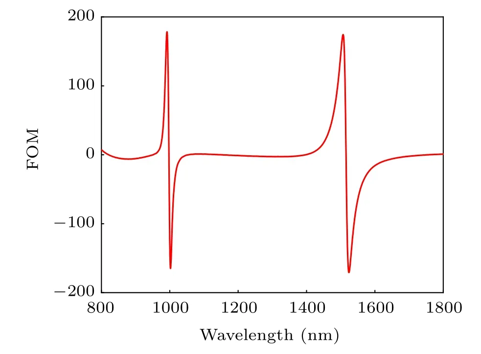
Fig.7. FOM varying with wavelength of the whole system.
4. Conclusion
In summary, the transmission characteristics of SPPs in a MIM waveguide coupled with Q-shaped resonator system are studied by FDTD method. The energy exchange between C1 and C2 leads to two distinct resonant dips in the system,as indicated by the simulation result, which is in high agreement with the MICMT result. Additionally, by adjusting the geometrical parametersL,wandR,the position of the two resonant dips can be adjusted independently. Moreover,the sensing characteristics of the proposed structure possess a good robustness in terms of the structural parameters. The sensitivity is consistently at a high level,up to 1578 nm/RIU.Obviously,sensor is designed in this work with high sensitivity, small size,excellent tunability and easy integration. Therefore,this work is a guidance for the design of nanoscale sensors and has a great potential in the application of the optoelectronic integration technology in the future.
Acknowledgments
This study is supported by the National Natural Science Foundation of China (Grant No. 61865008) and Northwest Normal University Young Teachers’ Scientific Research Capability Upgrading Program(Grant No.NWNU-LKQN2020-11).

- Chinese Physics B的其它文章
- Measurements of the 107Ag neutron capture cross sections with pulse height weighting technique at the CSNS Back-n facility
- Measuring Loschmidt echo via Floquet engineering in superconducting circuits
- Electronic structure and spin-orbit coupling in ternary transition metal chalcogenides Cu2TlX2(X =Se,Te)
- Characterization of the N-polar GaN film grown on C-plane sapphire and misoriented C-plane sapphire substrates by MOCVD
- Review on typical applications and computational optimizations based on semiclassical methods in strong-field physics
- Quantum partial least squares regression algorithm for multiple correlation problem