
First-principles study of stability of point defects and their effects on electronic properties of GaAs/AlGaAs superlattice
2022-03-12 07:48ShanFeng冯山MingJiang姜明QiHangQiu邱启航XiangHuaPeng彭祥花HaiYanXiao肖海燕ZiJiangLiu刘子江XiaoTaoZu祖小涛andLiangQiao乔梁
Chinese Physics B 2022年3期
关键词:海燕
Shan Feng(冯山) Ming Jiang(姜明) Qi-Hang Qiu(邱启航) Xiang-Hua Peng(彭祥花)Hai-Yan Xiao(肖海燕) Zi-Jiang Liu(刘子江) Xiao-Tao Zu(祖小涛) and Liang Qiao(乔梁)
1School of Physics,University of Electronic Science and Technology of China,Chengdu 610054,China
2Department of Physics,Lanzhou City University,Lanzhou 730070,China
Keywords: first-principles calculations,GaAs/Al0.5Ga0.5As superlattice,point defects,electronic properties
1. Introduction
Semiconductor superlattices(SLs),each consisting of alternating thin layers of two or more different semiconductors,exhibit unique properties and are widely used in novel optical and electronic devices.[1-4]Especially,the GaAs/AlAs SL has received wide attention in the applications of high electron mobility transistor (HEMT) and quantum cascade laser(QCL).[5-8]However, when the SL materials are used in irradiation environments such as aerospace field,[9]high energy physics field,[10]and nuclear physics field,[11]point defects may appear in GaAs/AlAs SL, resulting in the failure of the SL-based devices.[12,13]Thus, it is important to improve the performance of GaAs/AlAs SL structure under irradiation. Recently, Jianget al.carried outab-initiomolecular dynamics (AIMD) calculations to explore its behaviors under electron irradiation and confirmed the experimental observation that the radiation resistance of GaAs/AlAs SL is enhanced by the introduction of Ga into AlAs layer.[14,15]Besides the superior radiation resistance,the GaAs/AlxGa1-xAs SL is also a promising candidate for electronic materials in the HEMT and QCL. Takashet al.[16]have fabricated a high electron mobility transistor (HEMT) with selectively doped GaAs/n-AlxGa1-xAs heterojunctions, and compared its mobilities and transconductance with those of GaAs MESFETs(MESFETs stand for conventional Schottky-gate field effect transistors). They found that the Hall mobility and transconductance of the HEMT at 77 K are 5.5 and 3 times higher than the corresponding values of the MESFETs, respectively,and the GaAs/n-AlxGa1-xAs HEMT has extremely high-speed microwave capability.[16]In the meantime,Hosakoet al. fabricated GaAs/AlGaAs and GaSb/AlSb tetrahertz quantum aascade lasers(THz-QCL)by using a resonant longitudinal optical(LO)phonon depopulation scheme. They reported that the GaAs/AlGaAs THz-QCL has a high peak power(close to few tens of milliwatts)operation and a high operating temperature(approximate to 123 K).[17]
Thus far, a number of investigations have been carried out on GaAs/AlxGa1-xAs materials to explore their optical and electronic properties.[18,19]Billaha and Das have investigated the effects of Si dopant on the physical properties of GaAs/AlxGa1-xAs-based quantum well infrared photodetector (QWIP),[20]and they found that the peak responsivity of the QWIP increases nonlinearly with the concentration of Si dopant increasing, and the peak absorption shifts toward the short wavelengths with the mole fraction of Al increasing. Goryachevaet al. have studied the optical transitions of GaAs/Al0.45Ga0.55As SL at room temperature by photoreflectance spectroscopy and determined the band gap of the SL structure to be 1.5 eV.[21]Theoretically, Klos and Krawczyk calculated the band structure of GaAs/AlxGa1-xAs SL and estimated the ultimate efficiency of SL-based solar cells,[22]and they found that the conversion efficiency of the SL structure is higher than that of its bulk components. Besides, Billaha and Das performed the AIMD simulations to investigate the electronic spectrum of n-type GaAs/AlxGa1-xAs heterojunction and found thatδ-doping can improve the mobility of electrons.[23]
Until now, the behaviors of GaAs/AlxGa1-xAs SL under irradiation environment have received relatively less attention. Expect for the studies of Jianget al.,[14,15]Nobuyukiet al. have investigated the effects of electron irradiation on the optical and electrical properties of GaAs/AlxGa1-xAs heterostructures in an energy range between 5 keV and 25 keV and at electron doses of (1×10¹⁶-1×10²¹) electrons/cm2,[24]and they proposed that electron irradiation induces degradation in both the optical properties and the electrical properties and observed that the most pronounced degradations happen at the energy of 10 keV.Laiadiet al.used the numerical simulations to compare the effect of electron irradiation with that of proton irradiation on the current-voltage characteristics of the GaAs/AlxGa1-xAs-based solar cell,[25]and they found that the electron irradiation and the proton irradiation cause their conversion efficiencies to decrease by 5.23% and 5.60%, respectively.
Despite the studies of the optic-electronic properties and the radiation resistance of GaAs/AlxGa1-xAs SL reported in the literature,the stability of point defects and their effects on the electronic properties of GaAs/AlxGa1-xAs SL are still unknown. Motivated by these considerations,we employ density functional theory(DFT)calculations to investigate the stability of point defects in GaAs/AlxGa1-xAs SL and their influences on the electronic properties, including band structures,density of state distributions, in this work. In the meantime,the carrier transport properties such as effective mass and carrier mobility are determined. The results provide an insight into the radiation damage effects of the superlattice semiconductors and also contribute to improving their performance under irradiation.
2. Computational details

Fig. 1. Schematic view of geometrical structures of (a) bulk GaAs, (b) ideal GaAs/AlAs SL, (c) ideal GaAs/Al0.5Ga0.5As SL, (d)-(i) defective GaAs/Al0.5Ga0.5As SL. XY (X,Y =Ga, Al or As): X occupying the Y lattice site; VX: X vacancy; Xint: X interstitial; Xint-VX: Frenkel pairs with third neighboring X interstitial. Yellow,purple,and pink spheres represent vacancy,interstitial,and antisite sites,respectively.

Fig.2. Schematic view of geometrical structures of optimized ideal and defective GaAs/Al0.5Ga0.5As SLs. XY (X,Y =Ga,Al or As): X occupying Y lattice site;VX:X vacancy;Xint:X interstitial;Xint-VX:Frenkel pairs with the third neighboring X interstitial. Yellow,purple,and pink spheres represent vacancy,interstitial,and antisite sites,respectively.
All the calculations are carried out by employing the density functional theory (DFT) and projector-augmented wave (PAW) method as implemented in the Viennaab-initiosimulation package (VASP).[26,27]The generalized gradient approximation (GGA) in the Perdew-Burke-Ernzerhof(PBE)[28]functional is used to describe the exchangecorrelation energy between electrons. The plane wave kineticenergy cutoff is set as 500 eV, and Monkhorst-Packk-point mesh is set to be 6×6×6. The convergence criteria for total energy and force are 10-5eV and 10-5eV/°A,respectively.Previous study has demonstrated that GaAs/Al0.5Ga0.5As SL structure may behave more robust than GaAs/AlAs SL.[14,29]In this study, the GaAs/Al0.5Ga0.5As SL, which consists of two monolayers of GaAs alternating with two monolayers of Al0.5Ga0.5As, is considered. The structure of GaAs crystal,which is similar to that of AlAs and belongs toTdpoint group of zinc blende, is shown in Fig. 1(a). Figures 1(b) and 1(c)show the geometrical structures of the ideal GaAs/AlAs SL and GaAs/Al0.5Ga0.5As SL,respectively.
As for the defective states, the considered point defects,including antisite, interstitial and vacancy, are based mainly on our previousab initiomolecular dynamics simulation of the radiation damage effects of GaAs/AlGaAs superlattice,[14]in which a number of point defects are revealed and their stability are investigated. For Ga,Al,and As Frenkel pairs(FPs),the FPs with the first, second, and third-nearest neighbor interstitials have been considered. However, all FPs with the first and second-nearest neighbor interstitials are not stable,and the recombination between vacancy and interstitial occurs. Meanwhile, FPs with the third-nearest neighbor interstitials are found to be stable, which are thus selected for the subsequent calculations. Besides, this study mainly focuses on the effects of the point defects that are close to the interface of the GaAs/Al0.5Ga0.5As superlattice on the electronic properties of the material. Schematic views of the considered point defects are illustrated in Figs.1(d)-1(i).The geometrical structures of these defects after structural relaxation are presented in Fig.2.It can be seen that the equilibrium geometrical structures of these defective SLs remain crystalline and there is no obvious deformation, suggesting that the introduced point defects affect the structural stability of the GaAs/Al0.5Ga0.5As SLs slightly.
3. Results and discussion
3.1. The ground state properties of bulk GaAs, bulk Al0.5Ga0.5As,and GaAs/Al0.5Ga0.5As SLs
The lattice constants of GaAs, Al0.5Ga0.5As, and GaAs/Al0.5Ga0.5As SLs are determined and shown in Table 1.From the table it follows that the optimized lattice constants of GaAs and Al0.5Ga0.5As are 5.609 °A and 5.623 °A, respectively, which agree well with the available experimental values (5.608 °A for GaAs[30]and 5.703 °A for Al0.5Ga0.5As[31])and theoretical values(5.653 °A for GaAs.[32]and 5.648 °A for Al0.5Ga0.5As[33]). It is noted that the lattice mismatch between GaAs and Al0.5Ga0.5As is as small as 1.443%.Thus,the medium value of 5.620 °A is used to build the structural model for GaAs/Al0.5Ga0.5As superlattice and a 2×2×2 supercell is then used. Subsequently,structural relaxation is carried out and the optimized supercell size of GaAs/Al0.5Ga0.5As superlattice is 11.228 °A×11.228 °A×11.228 °A, which is large enough to avoid the interaction between the defect and its periodic images.
The band structures of GaAs, Al0.5Ga0.5As and GaAs/Al0.5Ga0.5As SL are then calculated as shown in Fig.3.In all cases both the conduction band minima(CBM)and valence band maxima (VBM) are located atΓpoints, indicative of the direct character of band gap. Furthermore, the band gap of GaAs and Al0.5Ga0.5As are determined to be 0.52 eV and 1.13 eV, respectively, agreeing well with other theoretical results of 0.54 eV[34]and 0.86 eV,[31]respectively.The discrepancy between our results and the experimental values (1.52 eV for GaAs[32]and 2.09 eV for Al0.5Ga0.5As[35])can be attributed to the limitation of the DFT calculations,i.e., the DFT calculations generally underestimate the band gap of semiconductor materials due to the approximation of exchange-correlation functional in DFT method.[36]Besides,we find that the band gap of 1.13 eV for bulk Al0.5Ga0.5As is larger than the value of 0.52 eV for GaAs. These results are consistent with the results of Degheidyet al.,who found that the band gap of Al0.5Ga0.5As is larger than that of GaAs and smaller than that of AlAs.[37]As for GaAs/Al0.5Ga0.5As SL,its direct band gap was calculated to be 0.84 eV. Goryachevaet al. have measured the band gap of GaAs/Al0.45Ga0.55As SL to be 1.50 eV,[21]which is larger than our result.

Table 1. Calculated values of lattice constant(a)and band gap(Eg)of bulk GaAs and Al0.5Ga0.5As and available experimental and theoretical results.

Fig.3. Band structures of(a)bulk GaAs,(b)bulk Al0.5Ga0.5As,and(c)GaAs/Al0.5Ga0.5As SL.The Fermi level is set to be 0 eV.
3.2. Formation energy of point defects in GaAs/Ga0.5Al0.5As SL


As shown in Table 2,the AsAl(As occupying the Al lattice site)and the AlGa(Al occupying the Ga lattice site)antisite defects have negative formation energy values of 0.03 eV and 0.46 eV under As-rich condition, respectively, indicating that their formation are exothermic process. For AsGa(As occupying the Ga lattice site) and GaAl(Ga occupying the Al lattice site)antisite defects,their formation energy values are determined to be 0.07 eV and 0.47 eV, respectively.Our calculations suggest that these antisite defects form easily in GaAs/Al0.5Ga0.5As SL under As-rich condition. Under cation-rich condition, the AlAs(Al occupying the As lattice site), GaAs(Ga occupying the As lattice site), AlGaand GaAlare more favorable than AsGaand AsAlantisite defects as indicated by their relatively small formation energy values of 0.14,1.02,-0.55,and 0.56 eV,respectively.

Table 2. Defect formation energy (in unit eV) of GaAs/Al0.5Ga0.5As SL under As-rich and cation-rich conditions. XY (X,Y =Ga,Al or As):X occupying Y lattice site; VX: X vacancy; Xint: X interstitial; Xint-VX: Frenkel pairs with the third neighboring X interstitial as shown in Figs.1(g)-1(i).
In the case of vacancy defects, theVAl(Al vacancy) andVGa(Ga vacancy)defects show similar stabilities as indicated by their similar formation energy values under both As-rich and cation-rich conditions. It is noted that theVAlandVGaare more energetically favorable thanVAsunder As-rich condition, while theVAsis more preferable thanVAlandVGaunder cation-rich condition. Besides, it is noted that the formation energy values for interstitial and FP defects are generally high as shown in Table 2. The preferable interstitial defects are found to be As and Ga interstitial under As- and Ga-rich conditions, respectively, and the respective formation energy values are 2.59 eV and 2.29 eV. For the FPs, it is found that they are difficult to form due to their relatively high formation energy values.
The defect formation energy values in GaAs/Al0.5Ga0.5As SL structure are plotted in Fig. 4. One can see from Fig. 4 that the AlGaantisite is the most favorable defect in GaAs/Al0.5Ga0.5As SL. Besides, except for the AlGaantisite,other antisite defects like AsGa,AsAl,GaAl,and GaAsare also favorable. Jianget al.employed an AIMD method to explore the radiation resistance of GaAs/Al0.5Ga0.5As SL.[14]Their studies showed that the antisite defects are generally easier to form under electron irradiation, which is consistent with our results. Figure 4 also shows that in most cases the stability of point defects depends on the chemical environment of chemical species. A similar phenomenon has been observed in other materials. In the literature, Xiaoet al. found that the stable chemical potential region for pure Cs2AgBiBr6is narrow,and the Br-poor/Bi-rich condition is preferred for suppressing the formation of the Bi vacancy and Ag-Bi antisite defects,which is beneficial for maximizing the photovoltaic performance.[45]Baierleet al. performed spin-polarized DFT calculations of the electronic and structural properties of vacancies and antisites in zigzag, armchair, and chiral SiC nanotubes, and reported that the formation energy for antisite defects in SiC nanotubes can be affected by the chemical potential of Si and C.[46]Shuet al. investigated the stability of various surface point defects in p-type-doped GaAs nanowires by the first-principles calculations. Their results suggested that As antisite (AsGa) is a highly stable surface point defect under As-rich condition,and reducing As chemical potential(or As partial pressure)is a feasible method to suppress the influence of AsGa defects on the p-type-doped GaAs nanowires.[47]

Fig. 4. Defect formation energy values of GaAs/Al0.5Ga0.5As SLs under As-rich and cation-rich conditions. XY (X,Y =Ga,Al or As): X occupying the Y lattice site;VX: X vacancy;Xint: X interstitial. Xint-VX: Frenkel pairs with the third neighboring X interstitial as shown in Figs.1(g)-1(i).
3.3. Effects of point defects on electronic properties of GaAs/Al0.5Ga0.5As SL
Considering the preferability of antisite defects in GaAs/Al0.5Ga0.5As SL, we explore their effects on the band structures of GaAs/Al0.5Ga0.5As SL first. Figure 5 shows the band structures of GaAs/Al0.5Ga0.5As SL with different types of antisite defects. For the AlAsand GaAsantisite defective states,their corresponding band structures are similar to each other,which may be due to the fact that the Al and Ga chemical elements have similar valence electronic configurations,i.e.,3s23p1for Al and 4s24p1for Ga. Comparing with the valence electronic configurations of As atom (4s24p3), we find that the formation of AlAsand GaAsantisite defects is accompanied by introduction of extra holes,i.e., p-type doping. As shown in Figs.5(a)and 5(d),the impurity levels cross the Fermi level and lead to the metallic character of the defective SL structures. When the AsAland AsGaantisite defects are created in GaAs/Al0.5Ga0.5As SL,more electrons are introduced. On the other hand, the Fermi levels shift from 3.14 eV for ideal SL to 3.77 eV and 3.86 eV for AsAland AsGaantisite defective states,respectively. These results suggest that the AsAland AsGaantisite defects act as donors in the GaAs/Al0.5Ga0.5As SL, indicative of n-type doping. Figures 5(b)and 5(c)show that the impurity levels are delocalized in the forbidden band, which may influence the carrier transport properties of GaAs/Al0.5Ga0.5As SL significantly.[48]The band structures for GaAland AlGaantisite defects are shown in Figs.5(e)and 5(f),respectively.

Fig.5. Band structures of GaAs/Al0.5Ga0.5As SL with(a)AlAs,(b)AsAl,(c)AsGa, (d)GaAs,(e)GaAl and(f)AlGa antisite defect. XY (X,Y =Ga,Al or As): X occupying the Y lattice site,The Fermi level is set to be 0 eV.
Owing to the similar valence electronic configurations of Al and Ga chemical elements, the AlGaand GaAlantisite defects show similar characters in band structures. Besides,they have slight effects on the shape of band structure and reduce only the band gap of GaAs/Al0.5Ga0.5As SL from 0.84 eV to 0.55 eV and 0.46 eV, respectively. It is noted that the defective SLs with GaAsand AlAsantisite defects show metallicity,while the defective SLs with AsAlAsGa, AlGa, and GaAlantisite defects still have the characters of semiconductor with the band gaps of 0.11 eV, 0.15 eV, 0.55 eV, and 0.46 eV, respectively. In order to further understand the effects of antisite defects on the electronic structure of GaAs/Al0.5Ga0.5As SL,the partial density of state (PDOS) distribution of the defective SL is plotted in Fig. 6. As shown in Fig. 6(a), the CBM of ideal GaAs/Al0.5Ga0.5As SL is mainly contributed by Ga-4s and Ga-4p orbitals,and the VBM is mainly contributed by As-4p orbitals. When the AlAsand GaAsantisite defects are introduced into the SL structure,the impurity levels cross the Fermi level,resulting in metallic character of the SL as shown in Figs.6(b)and 6(e). Besides, the impurity levels are found to be mainly contributed by the hybridization between As-4p orbitals and Ga-4p orbitals. As for the AsAland AsGaantisite defective states (see Figs. 6(c) and 6(d)), their band gaps decrease obviously,as compared with the value of ideal state.This is mainly due to the fact that the introduced point defects produce the impurity levels that are close to the VBM in the forbidden band. Meanwhile, the band gaps of AlGaand GaAldefective states(see Figs.6(f)and 6(g))decrease slightly,because the CBM shifts toward low energy level while the VBM remains nearly intact.
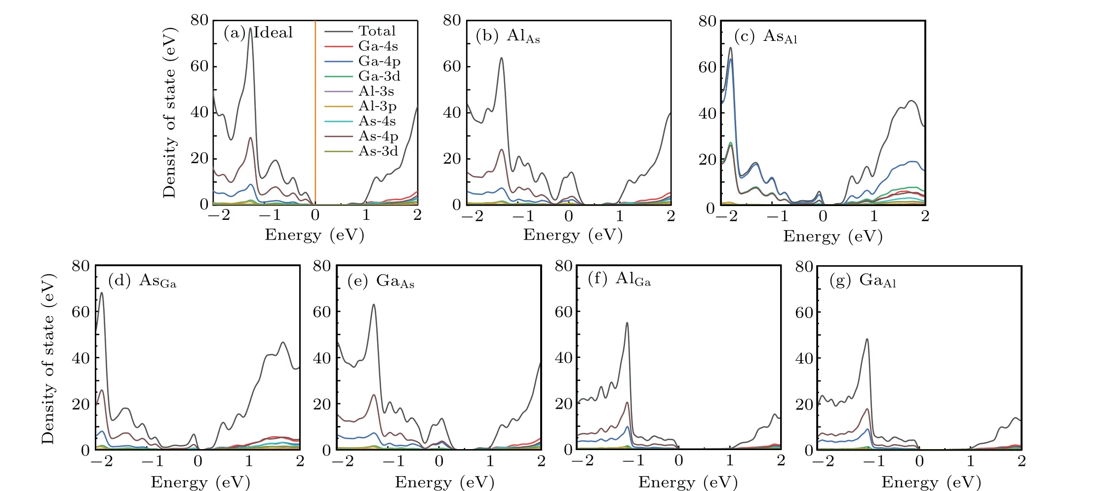
Fig.6. Partial density of state for(a)ideal and(b)-(g)defective GaAs/Al0.5Ga0.5As SL.XY (X,Y =Ga,Al or As): X occupying the Y lattice site. The Fermi level is set to be 0 eV.

Fig. 7. Band structures of GaAs/Al0.5Ga0.5As SL with (a) Asint, (b) Alint, (c) Gaint, (d)VAs, (e)VAl, and (f)VGa defect. VX (X =Al, Ga or As): X vacancy;Xint: X interstitial. The Fermi level is set to be 0 eV.

Fig.8. Band structures of GaAs/Al0.5Ga0.5As SL with(a)Gaint-VGa,(b)Asint-VAs,(c)Alint-VAl Frenkel pair defects. Xint-VX: Frenkel pairs with the third neighboring X interstitial as shown in Figs.1(g)-1(i). The Fermi level is set to be 0 eV.
The band structures of GaAs/Al0.5Ga0.5As SL with vacancy and interstitial defects are plotted in Fig.7. TheVAlandVGadefects can be regarded as p-type dopants,and the impurity levels cross the fermi level and affect the valence bands considerably as shown in Figs.7(a)and 7(b). In contrast,theVAsdefect shown in Fig.7(c)acts as an n-type dopant and the conduction bands are influenced considerably, for which the Fermi level is also crossed. We find that the nearest atoms around the vacancy defects are equally displaced toward the empty lattice site, which results in the charges transferring between atoms more easily,i.e., the shallow impurity levels caused by point defects will result in high concentration of the carriers in the SLs.[48]For the interstitial defects,the Alintand Gaintdefects act as n-type dopants, while the Asintdefect is regarded as a p-type dopant. As shown in Figs.7(d)-7(f),the impurity levels cross the Fermi level in all cases, indicating that the SLs with interstitial defects are metallic. The band structures of GaAs/Al0.5Ga0.5As SL with Ga,As,and Al FPs(see Figs. 1(g)-1(i)) are presented in Figs. 8(a)-8(c). In all cases, the impurity levels cross the Fermi level and lead to metallic characters.
There is no doubt that the introduced point defects modify the electronic structure of GaAs/Al0.5Ga0.5As SL significantly, and the defective SL structure generally is of metallic character, except for the AsAl, AsGa, AlGa, and GaAldefective states. In the meantime, although the AsAl, AsGa, AlGa,and GaAldefective SLs still remain semiconducting,their band gaps decrease significantly.
3.4. Effects of point defects on transport properties of GaAs/Ga0.5Al0.5As SL
The electron mobility at 0 K can be calculated from the equationμ=eτ/m*,[49]whereeis the electron charge,τis the relaxation time, andm*is the effective mass of carrier. The electron effective masses can be determined from the equation[49-51]

Here, ħ is the reduced Planck constant,kis the wave vector, andE(k) is the energy of CBM. According to Fig. 3(a),the electron effective mass of bulk GaAs is calculated to be 0.056me, which agrees well with the experimental value of 0.057me.[52]The relaxation time of 0.48 ps for bulk GaAs reported by Gonzalezet al.[53]is employed in this study.The electron mobility of bulk GaAs at 0 K is determined to be 1.501×104cm2/V·s, which is higher than the experimental value of 0.942×104cm2/V·s.[54]We also calculate the electron mobility of GaAs/Al0.5Ga0.5As SL to be 1.380×104cm2/V·s, which is larger than the value of 1.0×104cm2/V·s for GaAs/AlAs SL.[55]The results demonstrate that the GaAs/Al0.5Ga0.5As SL may have better performance than GaAs/AlAs SL in applications like HEMT, for which high carrier mobility is needed. Meanwhile, the hole mobility of GaAs/Al0.5Ga0.5As SL is also considered to make a comparison with that of p-type-doped defects,which is calculated to be 0.065×104cm2/V·s.
The corresponding electron or hole effective mass and carrier mobility for ideal and defective GaAs/Al0.5Ga0.5As SLs along theΓ-Xdirection have been summarized in Table 3. For the antisite defects, the AlAsand GaAsdefects act as acceptors while the AsGaand AsAldefects can function as donors in the defective GaAs/Al0.5Ga0.5As SLs. Comparing with the ideal state, the calculated electron effective mass for AsGaand AsAlincrease,and the electron mobility of GaAs/Al0.5Ga0.5As SL decreases from 1.38×104cm2/V·s to 1.154×104cm2/V·s and 1.214×104cm2/V·s, respectively. For the p-type-doped AlAsand GaAsdefects, they have positive effects on the hole mobility, since the calculated hole mobility of 0.122×104cm2/V·s for AlAsdefect and 1.21×104cm2/V·s for GaAsdefect are larger than the value of 0.065×104cm2/V·s for ideal state. In the case of AlGaantisite defects, the electron mobility is improved while the hole mobility decreases,but in the case of GaAlantisite defects, the electron mobility and hole mobility both decrease.As for the interstitial, vacancy and FP defects, the electron mobility of GaAs/Al0.5Ga0.5As SL decreases significantly due to the existence of these types of defects. On the other hand,the hole mobility of GaAs/Al0.5Ga0.5As SL also decreases except AsintandVAldefects, for which the hole mobilities are 0.153×104cm2/V·s and 0.114×104cm2/V·s, respectively.Our calculations show that the effects of point defects on the transport properties of GaAs/Al0.5Ga0.5As SL are generally negative, while the AlGaantisite defect enhances the electron mobility remarkably and the AlAs, GaAs, Asint, andVAldefects increase the hole mobility significantly. Considering the relatively high formation energy of AsintandVAldefects, we thus propose that introduction of AlAs,GaAs,and AlGaantisite defects into GaAs/Al0.5Ga0.5As SLs may be an effective strategy to improve the carrier mobilities of the SL-based devices.Since this study focuses mainly on the influences of interfacial point defects and the considered defects are all located in the vicinity of the interface of the GaAs/Al0.5Ga0.5As superlattice,the conclusion drawn in this work may be applicable to other(GaAs)m/(Al0.5Ga0.5As)n(m+n >2)superlattices.

Table 3.Calculated values of band gap(Eg),electron(positive value)or hole(negative value)effective mass(m*),and electron or hole mobility(μ)along Γ-X direction in Brillouin zone for GaAs/Al0.5Ga0.5As SL.XY (X,Y =Ga,Al or As):X occupying the Y lattice site;VX:X vacancy;Xint: X interstitial;Xint-VX: Frenkel pairs with the third neighboring X interstitial as shown in Figs.1(g)-1(i).
4. Conclusions
In summary, the stabilities of point defects in Ga0.5Al0.5As/GaAs superlattice and their effects on the electronic structure and transport properties of superlattice structure have been investigated by density functional theory calculations. The results show that the antisite defects are generally dominant under As-rich and cation-rich conditions, and the interstitial and FPs defects are much more difficult to form.The band structures of the GaAs/Al0.5Ga0.5As superlattice are modified significantly by most of the point defects, and the defective SLs are generally of metallic character except the AsGa, AsAl, AlGa, and GaAldefective states. The further calculations show that the electron or hole mobility of GaAs/Al0.5Ga0.5As superlattice is generally reduced due to the existence of point defects,while the AlAs,GaAs,and AlGaantisite defects, which can form easily in Ga0.5Al0.5As/GaAs superlattice, can improve the hole or electron mobility of the SL considerably. The results suggest that intentional introduction of AlAs, GaAs, and AlGaantisite defects can improve the carrier transport properties of GaAs/Al0.5Ga0.5As superlattice.
Acknowledgements
The theoretical calculations were performed using the supercomputer resources at TianHe-1 in the National Supercomputer Center in Tianjin.
Project supported by the NSAF Joint Foundation of China(Grant No. U1930120), the Key Natural Science Foundation of Gansu Province, China (Grant No. 20JR5RA211),and the National Natural Science Foundation of China(Grant No.11774044).
猜你喜欢
新农村(浙江)(2021年3期)2021-03-08
学校教育研究(2017年29期)2017-10-21
校园英语·下旬(2016年12期)2017-03-31
特别文摘(2016年8期)2016-05-04
特别文摘(2016年8期)2016-05-04
中国校外教育(下旬)(2014年9期)2014-11-11
红蜻蜓·低年级(2014年7期)2014-10-20
新高考·高三英语(2013年5期)2013-08-20
- Chinese Physics B的其它文章
- Measurements of the 107Ag neutron capture cross sections with pulse height weighting technique at the CSNS Back-n facility
- Measuring Loschmidt echo via Floquet engineering in superconducting circuits
- Electronic structure and spin-orbit coupling in ternary transition metal chalcogenides Cu2TlX2(X =Se,Te)
- Characterization of the N-polar GaN film grown on C-plane sapphire and misoriented C-plane sapphire substrates by MOCVD
- Review on typical applications and computational optimizations based on semiclassical methods in strong-field physics
- Quantum partial least squares regression algorithm for multiple correlation problem