
On the origin of the anomalous sign reversal in the Hall effect in Nb thin films
2022-03-12 07:44DanZhou周丹HanSongZeng曾寒松RujunTang汤如俊ZhihongHang杭志宏ZhiweiHu胡志伟ZixiPei裴子玺andXinshengLing凌新生
Chinese Physics B 2022年3期
关键词:新生
Dan Zhou(周丹) Han-Song Zeng(曾寒松) Rujun Tang(汤如俊) Zhihong Hang(杭志宏)Zhiwei Hu(胡志伟) Zixi Pei(裴子玺) and Xinsheng Ling(凌新生)
1Institute for Advanced Study School of Physical Science and Technology,Soochow University,Suzhou 215006,China
2Institute of Physics,Chinese Academy of Sciences,Beijing 100190,China
3Department of Physics,Brown University,Providence,Rhode Island 02912,USA
Keywords: anomalous sign reversal,Hall effect,edge supercurrents,Aharonov-Bohm effect
1. Introduction
In thin film superconductors, the transport properties associated with the resistive transition in a magnetic field have been of longstanding interests. An unresolved controversy is the origin of the anomalous sign reversal in the Hall effect,first debated in 1990s,[1-8]and it has generated great controversies recently.[9-11]Several possible mechanisms have been proposed.[2-6,10]However,in a study of disordered superconducting tantalum nitride films,[12]no such sign reversal was observed in the Hall effect across the resistive transition in a magnetic field. Thus it remains a mystery as to the origin of the observed anomalies in the Hall effect in the systems such effects have been observed.
In this study, we wish to re-visit this problem in sputtered niobium(Nb)thin films, a system that was investigated previously and an anomalous sign reversal in the Hall effect was observed under certain conditions.[7]Recently,it has been suggested[13,14]that much of the broadening in the resistive transition from the normal state to the superconducting state in sputtered Nb thin films is due to the surface superconductivity. Thus whether the previously observed anomalous sign reversal in the Hall effect is related to the surface superconductivity in this system is an unresolved question.
Edge or surface superconducting state was predicted long ago by Saint-James and de Gennes (SJdG)[15]and this effect has been confirmed in bulk samples with a flat surface that one can align the magnetic field with.[16,17]The surface superconductivity was also believed to play a role in the vortex physics in the bulk between upper critical fieldHc2(T) and surface nucleation fieldHc3(T).[18,19]For a thin film superconductor with a magnetic field applied normal to the film,the surface superconductivity effects have largely been ignored in the past. However, two recent experimental studies[13,14]clearly suggested that the broadened resistive transition can be,at least partially,attributed to the surface superconductivity of the crystalline Nb grains with their surfaces being parallel to the magnetic field.
Here we report an experimental study of the Hall effect and the magneto-resistive transition in sputtered Nb thin films.We find that, as previously reported,[7]there is indeed an observable sign reversal of the Hall effect across the normalsuperconducting transition as a function of the applied magnetic field. We find that this anomalous sign reversal in the Hall effect appears or disappears depending on a small change of the field orientation relative to the edge surface of the sample. A simple model is proposed that the anomalous sign reversal of the Hall effect may be caused by the edge surface supercurrents on the superconducting grains at the edges,due to the surface superconductivity.
2. Materials and methods
The materials used in this experiment are Nb thin films, of nominal thickness of 120 nm. The details of the Nb thin film deposition and characterization were described elsewhere.[20,21]As shown in Fig.1(a),the sample region consists of a 1 mm long horizontal channel with a width of 10 μm,the vertical lines are used for longitudinal and transverse voltage probes,with a width of 5 μm. The sample was patterned using standard photolithography and etched into the final form using the ion beam etching (IBE) process.[22]The surface of the Nb film Hall device was checked by the scanning electron microscopy (SEM), Figs. 1(a)-1(d). On the length scale above 100 nm,the film looks smooth and the IBE etched sample edges are sharp. However,below 100 nm,one can observe the poly-crystalline nature of the film, as shown in Fig. 1(d).We believe that the nanoscale roughness of the edges is the key to the understanding of the quantum transport of edge supercurrents. The transport measurements were carried out using the standard four-probe method with a commercial measurement system(Quantum Design PPMS-9). Alternating current directions were used to eliminate the thermal electric signals.
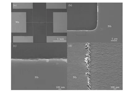
Fig.1. SEM micrographs of a patterned Nb thin film sample. (a)Whole sample,scale bar: 1.0 mm. (b)The expanded view of the small box region in(a);scale bar: 1.0 μm. (c)The expanded view of the small box region in(b);scale bar: 100 nm. (d)A close-up view of a part of an edge;scale bar: 100 nm.
The as-sputtered Nb thin-film sample used in this experiment has a superconducting transition temperature atTc=8.875 K in zero magnetic field. The superconducting transition temperature is defined as the temperature at which the sample resistance has decreased to 50% of the normal-state value at 10.0 K.Using the normal-state resistivityρxxat 10 K,we estimate the Drude mean free pathl= ¯hkF/ne2ρxxto be 18.5 nm,or about the grain size of the sputtered Nb films,see Fig.1.
3. Results and discussion
Figure 2 shows the longitudinal and transverse resistances for the superconducting-normal transition at 4.0 K,as a function of magnetic fieldH, atI=100 μA,T=4.0 K, and at three different angles between the sample and the magnetic field,as illustrated in the inset in Fig.2(a). The“no-rotation”configuration is when the magnetic field is perpendicular to the film(thus parallel to the edge surfaces,within 1°-2°). The longitudinal resistanceRxxand transverse resistanceRxyare defined asRxx=Vxx/IxandRxy=Vxy/Ix, respectively. Since the voltage signals due to the Hall effect change sign when the magnetic field direction is reversed,we plot both the symmetric and anti-symmetric parts ofRxxandRxy, as shown in Figs.2(a)-2(d).
Figure 2(a) shows the symmetric part ofRxx, (Rxx(H)+Rxx(-H))/2, which is the longitudinal resistance along the 1 mm long path. The transition from zero resistance superconducting state to the normal state is broad,over 3 kOe. We definedHc2as the steepest slope inRxx(H)andHc3as where the longitudinal resistance first starts to decrease (~1% change)from the normal state value. This broadened resistive transition in Nb attracted attention recently[13,14]with respect to the surface superconductivity. Tilting the sample with respect to the magnetic field has negligible effects in this longitudinal resistance.
However, as shown in Fig. 2(b), tilting the magnetic field has a drastic effect on the anti-symmetric part ofRxx,(Rxx(H)-Rxx(-H))/2. When the sample is tilted either aroundxoryaxis,Rxx(anti-symmetric) changes from two small peaks aroundHc2, for field normal to the sample, to a large peak as a function of the magnetic field when the sample is tilted by 10°, only tending to zero atHc3. The asymmetry effect of the sample geometry imperfection is small in our device and is not the cause of the effect here.
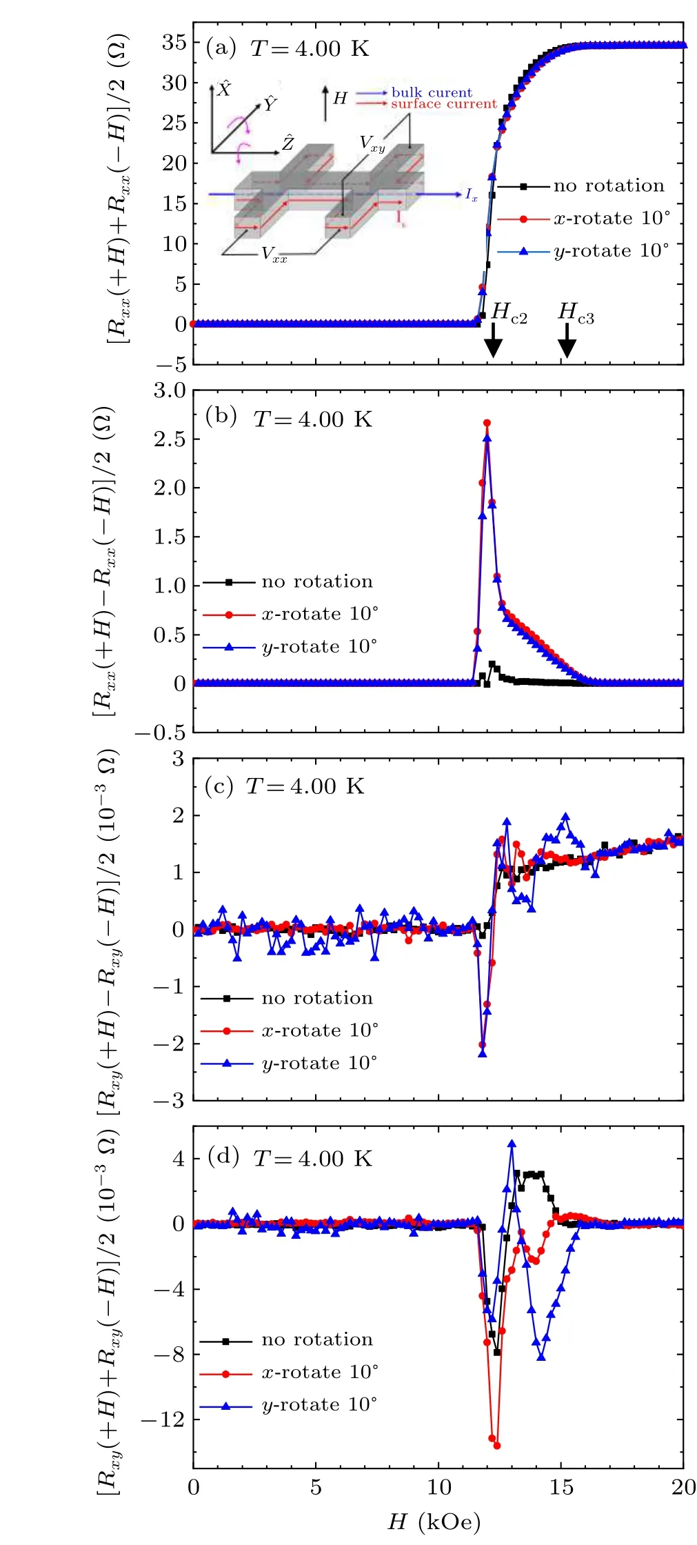
Fig.2.Magnetic field dependence of longitudinal and transverse resistances.(a) The symmetric part of the longitudinal resistance Rxx. (b) The antisymmetric part of the longitudinal resistance. (c) The Hall resistance, the anti-symmetric part of the transverse resistance. (d)The symmetric part of the transverse resistance. I=100 μA,T =4.0 K.
The anti-symmetric part of the transverse resistance,Rxy, (Rxy(H)-Rxy(-H))/2, is the Hall effect, as shown in Fig.2(c). When the magnetic field is perpendicular to the film surface, with decreasing field, the Hall resistance is a linear function of the magnetic field down toHc2where it drops to zero, with no sign change. However, when the sample is rotated by 10°,either aroundx-axis ory-axis,(see Fig.2(a)inset for clarity), there are oscillatory behaviors in the Hall resistance. The Hall resistance clearly changes sign atHc2. Similar oscillatory behavior inRxywas reported in Ref. [7], but was erroneously attributed to the vortex pinning behavior in the vortex state since theHc3was misidentified as theHc2.
The symmetric part of the transverse resistanceRxyis resistive since it is due to a longitudinal voltage developed along the direction of the current. Figure 2(d) shows large oscillations as a function of the magnetic field for all three field configurations. To be discussed in detail below, we believe these oscillations are due to the Aharonov-Bohm interference effects around the nanoscale grains on the edges of the voltage probes.
A simple way to test if the anomalies in Fig. 2 are due to the surface superconductivity is to check how they depend on the amplitudes of the applied currents. The surface superconducting layer cannot support a large current since it flows within a thin region of the size of the coherence length and it is limited by the depairing current density. Figure 3 shows the effects of the applied current inRxyvs.H. We find that the anomalous effects in Fig.2 are extremely sensitive to the magnitude of the applied current. For clarity, the anti-symmetric(Hall effect) and the symmetric parts (resistive) ofRxydata are plotted in an expanded view, zooming into the transition region. With decreasing field, whenHc3is crossed, the antisymmetric part ofRxyshows the normal Hall effect and drops to zero atHc2,while the symmetric part ofRxyexhibits a large increase at low currents 100-200 μA,this effect is suppressed at 500 μA, demonstrating that these features are indeed surface current effects.
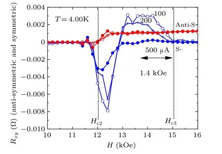
Fig.3.Effects of applied current:anti-symmetric(red,Hall effect)and symmetric parts(blue,resistive)of the transverse resistance Rxy,at T =4.00 K,I = 100, 200, 500 μA. Rxy(Anti-S) = (Rxy(H)-Rxy(-H))/2, Rxy(S) =(Rxy(H)+Rxy(-H))/2. Open circles, crosses, and solid circles are for 100 μA,200 μA,and 500 μA respectively. The 100 μA data are the same as the“no rotation”in Fig.2 for reference.
The next question is how these anomalous behaviors change with increasing temperature. Figure 4 shows the magnetic field dependence of the transverse resistance at 4-9 K.Two major features can be discerned immediately. First we notice that the oscillatory behavior betweenHc2andHc3fades away with increasing temperature. Second, which is a surprise,the symmetric part ofRxychanges abruptly from a large negative peak nearHc2to a large positive peak,when temperature is increased from 5 K to 6 K,then back to a negative peak again from 7 K to 8 K.This behavior cannot be explained by the pinning behavior in the vortex state, as often attributed to in the literature.[2-4,7,9,11]It can be easily accounted for in the model we present below.

Fig.4. Magnetic field dependence of transverse resistance Rxy at temperature(a)4 K,(b)5 K,(c)6 K,(d)7 K,(e)8 K,(f)9 K,respectively. For this sample,the zero-field Tc(half normal-state resistance)=8.875 K.The anti-symmetric part is the Hall resistance,the symmetric part is the anomaly discussed in the text.
4. Model: edge supercurrent loops
In Fig.5,we propose a simple model that provides a qualitative explanation for all of the observations here. Our model is based on the following observations. First, the resistance oscillations in Figs.2 and 3 have a period of ΔH~1.4 kOe(as marked in Fig.3). This field interval corresponds to a change of one flux quantum(ΔΦ=2.07×10⁻⁷G·cm2,in CGS units)in the cross-sectional area of 1.48×10⁻¹⁰cm2,or(120 nm)2.This suggests that the source of current loops is on the scale of 120 nm,not due to the current loop around the entire sample.We should emphasize that the signal is not a simple sinusoidal function of the magnetic field, the data show large variations with the magnetic field. We envision that each grain has its own oscillatory dependence and what we observed is an additive effect of many Aharonov-Bohm oscillations.
Second, a close examination of the SEM micrographs(Fig.1(d))will convince us that on the scale of~100 nm,the Nb film edges are quite rough. Since an Aharonov-Bohm ring attached to a 1D conduction channel can change the transmission rate in the channel,[23]given the poly-crystalline nature of the sputtered Nb films,it is reasonable to assume that there are many 100 nm scale grains along the edges that are capable of acting as microloops of supercurrents with Aharonov-Bohm interference effects, which will result in a modulation of resistance in a constant current measurement. In Fig.5,we draw two such nanoscale particles, or grains, for illustration.Since clearly there is a distribution of grain sizes,one expects a distribution of Aharonov-Bohm periodicities. After a closer examination of the curves in Fig.3 one can see that the modulation effects of multiple periods in magnetic field are indeed visible.
We should point out that the Drude mean free path of the normal-state electrons in this sample is of the order of 18.5 nm,thus the observed field-dependent resistance oscillations cannot be due to the phase-sensitive behavior of the normal electrons. The fact that the effects occur betweenHc3andHc2strongly suggests that it is caused by the surface supercurrents.Recently Aleineret al.[24]discussed the possibility of this behavior.
The first anomaly that can be accounted for by the model in Fig. 5 is the anomalous peak in the anti-symmetric part of the longitudinal resistanceRxx, as shown in Fig. 2(b). This is a pseudo Hall effect. It is larger than the real Hall effect,in Fig. 2(c), by 3 orders of magnitude. Thus it cannot be explained by the imperfection in the Hall probe geometry. It can be naturally explained if we realize that there is a diamagnetic surface current(the blue dashed lines in Fig.5)due to the edge surface superconductivity, as it is implied in the SJdG theory.[15]This SJdG diamagnetic current reverses direction when the external magnetic field is reversed. Thus the edge currents on theL1andL2paths are not equal. This inequality in edge current changes sign when the field is reversed, resulting in a pseudo Hall effect,the antisymmetric signal in the longitudinal resistanceRxx.
It should be noted that the diamagnetic current in the SJdG surface superconductivity theory is an equilibrium diamagnetism, not the induced screening current due to a field change. This can be tested by comparing the results for fieldincreasing and field-decreasing runs. Our results(not shown)show that they are identical,i.e.,reversible,thus ruling out this scenario.
The model in Fig.5 also offers a self-consistent explanation for the oscillations observed in the transverse resistanceRxy. The anti-symmetric part ofRxy, Fig.2(c), is the Hall effect; the symmetric part ofRxy, Fig. 2(c), is a longitudinal,resistive signal, a voltage along the current path. For magnetic field normal to the film,the“no rotation”mode,with decreasingH,the Hall resistance follows the normal state value(~H)down toHc2where it drops to zero with no sign change.However,the symmetric part ofRxyexhibits large oscillations,starting atHc3and ended atHc2, with decreasing magnetic field. When the sample is rotated by 10°, around eitherxaxis ory-axis,large oscillations appear in both anitisymmetric(Hall)and symmetric(resistive)parts ofRxy. These anomalies can easily be explained if we assume there is a nanoscale grain,which can support an Aharonov-Bohm current loop, on the edge ofC1edges of theCvoltage probe. Combined with the diamagnetic current that changes sign when the magnetic field is reversed, it is easy to see that an Aharonov-Bohm effect modulated resistance will give rise to both a pseudo Hall effect and a longitudinal resistance signal in theRxy. In our model,the anomalous sign reversal of the Hall effect in Fig.2(c)is a pseudo Hall effect due to the edge supercurrent,it has the same origin as the anomalous peak in the anti-symmetric part ofRxxin Fig.2(b),i.e.,the diamagnetic current due to surface superconductivity which breaks the symmetry in the edge currents on the opposing edges of the sample.
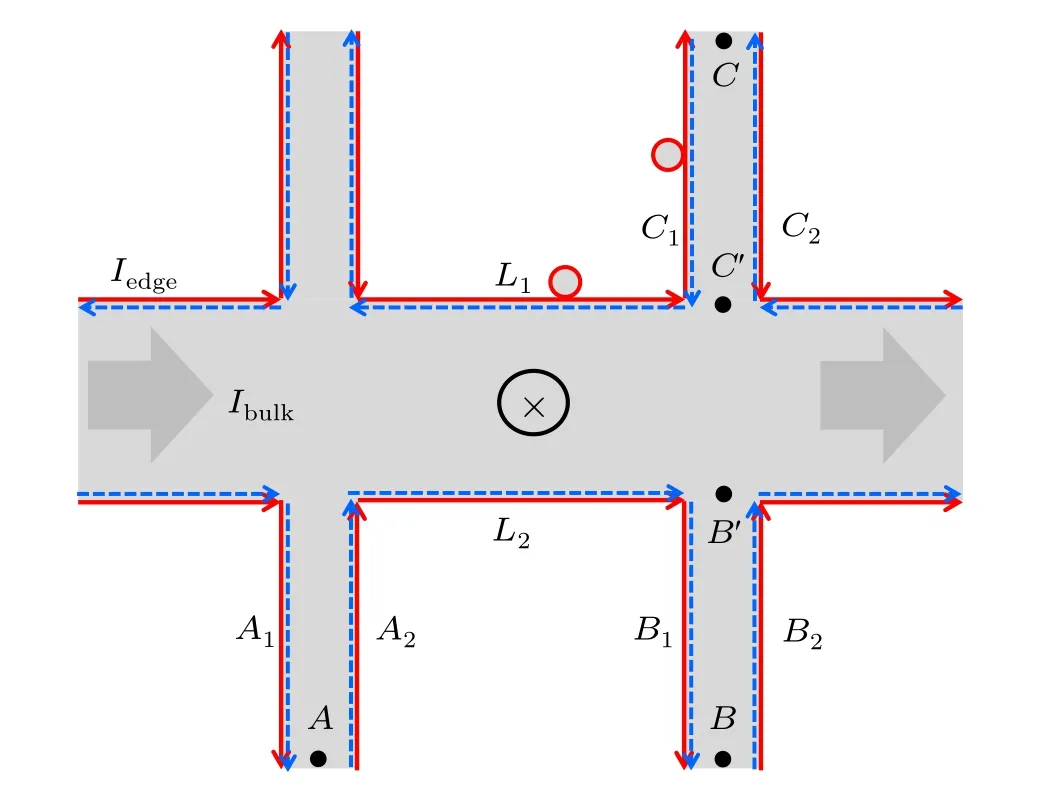
Fig. 5. A qualitative model of edge supercurrents in a Hall bar geometry with nanoscale grains,attached on the C1 side of transverse voltage probe C and on the L1 side of the main channel(not to scale). The applied current is from the left terminal to the right.When the applied field is between Hc2 and Hc3,the bulk normal current flows from left to right through the horizontal channel. The red lines are the edge supercurrent from the current source,the blue dashed lines are the diamagnetic current induced by the magnetic field in the surface superconducting state. The diamagnetic currents reverse directions when the external magnetic field is reversed. In contrast,the edge currents due to the applied current do not change directions when the magnetic field is reversed.
Finally,our model can account for the temperature dependence data in Fig.4 as well. As shown in Fig.4,with increasing temperature, most of the resistance oscillations betweenHc2andHc3disappear, as expected for the Aharonov-Bohm effect since the surface current loses its phase coherence. The change from a large negative peak to a positive peak,in Fig.4,can be understood if we consider the temperature dependence of the superconducting coherence length. With the coherence length increasing, the effective size of the superconducting particles will be changing. Effectively, the local current loop inC1may disappear and new ones may emerge on the edge ofB1. When that happens, the symmetric part of the voltage between probesBandCwill change sign.
5. Conclusions
In summary, we have re-visited the anomalous sign reversal problem in the Hall effect in the system of sputtered Nb thin films. We find that the anomalous sign reversal in the Hall effect is extremely sensitive to a small tilting of the magnetic field and to the magnitude of the applied current.Large anomalous variations are also observed in the symmetric part of the transverse resistanceRxy. We suggest that the observed anomalies may be accounted for if there are surface current loops on superconducting grains at the edges of the superconducting thin films. We should point out that our data are consistent with the simple model proposed in Fig. 5, but they are not definitive proof. An ideal experimental proof of the proposed model in Fig.5 would be using amorphous films and lithographic techniques to create a structure as shown in Fig. 5. With such a structure, one can directly correlate the Aharonov-Bohm effect with the diameter of the islands.
Acknowledgments
We are grateful to Professor X.G.Qiu for providing the Nb thin film samples. X. S. L. wishes to thank Professors P.Ao,D.E.Prober and J.Ye for helpful discussions and comments.This work was partially supported by the National Natural Science Foundation of China (Grant No. 51772200) (PI:R.J.Tang).
猜你喜欢
科教新报(2022年8期)2022-04-08
中国慈善家(2022年1期)2022-02-22
文艺生活·上旬刊(2021年8期)2021-09-18
文艺生活(艺术中国)(2021年8期)2021-09-18
北广人物(2020年21期)2020-06-01
汽车观察(2018年10期)2018-11-06
读者(2018年15期)2018-07-18
海峡姐妹(2017年7期)2017-07-31
视野(2015年4期)2015-07-26
中国记者(2014年1期)2014-03-01

- Chinese Physics B的其它文章
- Measurements of the 107Ag neutron capture cross sections with pulse height weighting technique at the CSNS Back-n facility
- Measuring Loschmidt echo via Floquet engineering in superconducting circuits
- Electronic structure and spin-orbit coupling in ternary transition metal chalcogenides Cu2TlX2(X =Se,Te)
- Characterization of the N-polar GaN film grown on C-plane sapphire and misoriented C-plane sapphire substrates by MOCVD
- Review on typical applications and computational optimizations based on semiclassical methods in strong-field physics
- Quantum partial least squares regression algorithm for multiple correlation problem