
Analysis of the generation mechanism of the S-shaped J-V curves of MoS2/Si-based solar cells
2022-03-12 07:44HeJuXu许贺菊LiTaoXin辛利桃DongQiangChen陈东强RiDongCong丛日东andWeiYu于威
Chinese Physics B 2022年3期
He-Ju Xu(许贺菊) Li-Tao Xin(辛利桃) Dong-Qiang Chen(陈东强)Ri-Dong Cong(丛日东) and Wei Yu(于威)
1College of Science,North China University of Science and Technology,Tangshan 063009,China 2College of Physics Science and Technology,Hebei University,Baoding 071002,China
Keywords: MoS2/Si-based solar cell,S-shaped J-V curve,power conversion efficiency,p+layer
1. Introduction
Transition-metal dichalcogenides (TMDs) have attracted increasing attention due to their rich electrical and optical properties.As typical TMD materials,MoS2films have strong optical absorption characteristics and high carrier mobility,and exhibit unique photoelectric characteristics that make them suitable for use in MoS2/Si-based solar cells.
In previous studies,[1,2]MoS2films were fabricated via the sol-gel method, and MoS2/Si-based solar cells were successfully prepared. The introduction of the MoS2film improved the performance of the solar cells and enabled them to obtain a conversion efficiency of 4.6%. However, an SshapedJ-Vcurve was observed, which exhibited nonideal p-n junction rectification characteristics. The S-shapedJ-Vcurve attenuates the output characteristic parameters, such as the open circuit voltage(VOC),the short circuit current density(JSC),and the fill factor(FF),which affects the conversion efficiency of the solar sell. Therefore, studying the generation mechanism of the S-shapedJ-Vcurve and improving the Sshape are beneficial for improving the conversion efficiency.Research into the generation mechanism of the S-shapedJ-Vcurve has attracted widespread attention.[3-9]Carabeet al.[3]proposed that non-ohmic contacts at the back interface of the heterojunction cause the formation of an S-shapedJ-Vcurve.Wanget al.[4]further analyzed the S-shapedJ-Vcurve generation mechanism of the non-ohmic contacts at the back of the heterojunction and reported that the size of the back contact barrier influences the formation of the S-shapedJ-Vcurve.The physical correlation between the electrical property degradation of the hole-selective layer and the generation of an SshapedJ-Vcurve in an inverted organic solar cell was analyzed by Ren´e Kogleret al.[5]Liuet al.[9]proposed that interface engineering was crucial for the development of efficient solar cells and consequently, the power conversion efficiency was enhanced from 7.5%to 15.5%.
In this study,a MoS2film is introduced into the front interface of the solar cell to analyze the generation mechanism of the S-shapedJ-Vcurve, and a p-n heterojunction is formed,enhancing theVOCand FF of the solar cell and improving the S-shape of theJ-Vcurve. The introduction of a p+layer into the back interface of the solar cell reduces the back contact barrier of the solar cell and eliminates the S-shape of theJ-Vcurve,achieving high power-conversion efficiency.
2. Experiment
2.1. Preparation
Figure 1(a)shows a structural diagram of a primitive solar cell,which is referred to as sample 1. Figures 1(b)and 1(c)show diagrams of a solar cell with an MoS2film at the front interface and a cell with a MoS2film at the front interface and a p+layer at the back interface,called sample 2 and sample 3,respectively. The details of the preparation of the MoS2thin films,ITO,and Ag electrodes were presented in our previous work.[1]A p+layer was prepared in the chamber of a PECVD deposition system at a deposition temperature of 300°C, a power of 21 W,and a working pressure of 253.3 Pa. The flow rates of SiH4, H2, CO2, and B2H6were 1.3 sccm, 201 sccm,1.0 sccm,and 0.54 sccm,respectively,and the deposition time was 20 min.

Fig.1. Structure diagram of(a)sample 1,(b)sample 2,and(c)sample 3.
A scanning electron microscopy (SEM) image of the cross section of sample 3 is shown in Fig.2,in which the presence of Si, ITO, and Ag can clearly be identified. However,the thickness of the MoS2layer is less than 10 nm, and we could not confirm the presence of the MoS2layer using the SEM cross-sectional image.

Fig.2. SEM image of the cross section of sample 3.
2.2. Characterization
A semiconductor device parameter analyzer (Agilent B1500A) was used at room temperature to measure theJ-Vcurves in the dark and under AM 1.5 illumination, as well as the capacitance-voltage(C-V)curves. The external quantum efficiency(EQE)was measured using the equipment described in our previous work.[1]
3. Results and discussion
The structure and quality of the MoS2film were analyzed via XRD,Raman spectroscopy,and XPS measurements in our previous work.[1]The results indicate that the MoS2film was successfully prepared. Figures 3(a)and 3(b)present theJ-Vcurves of samples 1-3 under AM 1.5 illumination and dark conditions. The photovoltaic parameters of the three samples are listed in Table 1 and it can be observed that the photovoltaic performances of the three samples gradually improve.VOCfirst increases from 116 mV to 236 mV, and then to 328 mV;JSCfirst increases from 31.73 mA·cm-2to 34.49 mA·cm-2,and then to 37.21 mA·cm-2;the FF first increases from 0.30 to 0.57, and then to 0.62; finally, the CE first increases from 1.1% to 4.6% and then to 7.55%. A p-n heterojunction is formed in the sample 2 due to the introduction of MoS2, producing a larger built-in electric field and a wider depletion region. The photo-excited carriers are effectively separated,[10]resulting in an increase inVOCandJSC.The serial ohmic loss and the ohmic shunt decrease due to the passivation effect of the MoS2film on the interface and the high conductivity of the p+layer, which improves theVOC,JSC,and FF.The shape of theJ-Vcurve also changes. TheJVcurves of samples 1 and 2 are both S-shaped; however, the shape of theJ-Vcurve of sample 2 is clearly improved,while the S-shape of theJ-Vcurve of sample 3 is eliminated and is similar to that of an ideal diode.
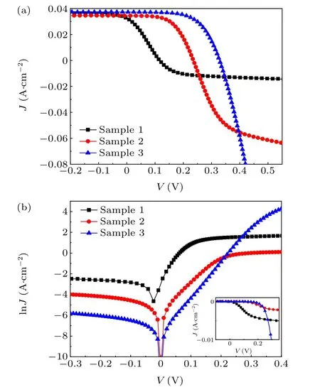
Fig.3. (a)The J-V curves under AM 1.5 illumination,(b)lnJ-V curves,the inset are J-V curves under dark conditions for samples 1-3.
The ideal factor,n,is extracted from Fig.3(b),as shown in Table 1.[1]The ideal factors of samples 1-3 are 1.63,1.45,and 1.10,respectively,implying an improvement in the performance of the samples due to the introduction of the MoS2film and the p+layer.

Table 1. Photovoltaic parameters of samples 1-3.

Fig.4. Energy level diagrams of(a)sample 1,(b)sample 2,and(c)sample 3.
An energy-level diagram of sample 1 is shown in Fig.4(a). The work functions of ITO,p-Si,and Ag are 4.5 eV,4.9 eV, and 4.3 eV, respectively. Electron transfer from ITO to p-Si occurs at the interface between the ITO and the p-Si,forming a space region of negative charge and a Schottky barrier through the downward energy band. Similarly, a Schottky barrier is formed at the interface between the p-Si and the Ag,resulting in two back-to-back Schottky barriers. A photovoltage is generated at the ITO/p-Si Schottky junction in the measurements of theJ-Vcurves under AM 1.5 illumination,which is equivalent to applying a positive bias voltage to the p-Si/Ag Schottky junction. The direction of the external bias voltage is opposite to that of the photovoltage,which is equivalent to applying a negative bias voltage to the p-Si/Ag Schottky junction. The external bias voltage varies continuously during the measurements. When the external bias voltage is much lower than the photovoltage,the p-Si/Ag Schottky junction is positively biased,and the positive resistance is minimal.Therefore, the effect of the Schottky junction on the current density is minimal and almost negligible. When the external bias voltage is close to the photovoltage,the forward bias voltage is too small,and the resistance cannot be ignored,resulting in a decrease inJSCand the FF.VOCalso decreases because of the voltage divided by the p-Si/Ag Schottky junction. When the external bias voltage is higher than the photovoltage,the p-Si/Ag Schottky junction is reverse biased,and the current density approaches the reverse saturation current density with increasing external voltage,instead of increasing exponentially.Thus,the S-shapedJ-Vcurve appears,as shown in Fig.3(a).
Figure 4(b)shows the energy level diagram of sample 2.When ITO comes into contact with MoS2,an electron transfer occurs from ITO to MoS2,forming a space region of negative charge at the interface between the two layers and an ohmic contact through the downward energy band. Sample 2 is a series device which is equivalent to a p-n junction and a p-Si/Ag Schottky junction in series. The p-n junction forms a larger built-in electric field and exhibits a wider depletion region width than the ITO/p-Si Schottky junction of sample 1,which improves theVOCand FF.However,the p-Si/Ag Schottky junction takes part of the voltage when the external bias voltage is close to the photovoltage,and is then reverse-biased when the external bias voltage is greater than the photovoltage. Therefore, the S-shapedJ-Vcurve is still observed, as shown in Fig.3(a),due to the existence of a p-Si/Ag Schottky junction.
Figure 4(c)shows the energy-level diagram of sample 3.The barrier width of the interface between the Ag and p+layers is relatively thin, due to the high doping concentration of the p+layer. Therefore, electrons can pass through the barrier region due to the tunneling effect,generating a large current and making an ohmic contact. Additionally, a high-low junction is formed between the p+layer and the p-Si. Consequently, the S-shapedJ-Vcurve is eliminated, as shown in Fig.3(a), and a higher output current density is obtained at a high voltage,compared to those of the other two solar cells.
Figure 5 presents the EQE spectra of the three samples,which show that the EQE values gradually increase.The width of the depletion region of sample 2 increases due to the introduction of the MoS2film,leading to an increase in the collection depth of the carriers and an improvement in the EQE.[11]An ohmic contact is formed between the p+layer and the Ag electrode due to the introduction of the p+layer, and a high-low junction is formed between the p+layer and the p-Si; these are more conducive to carrier transport. Therefore,the short-circuit current density is increased, and the EQE is further improved.
Figure 6 shows theC-Fcurves of the three samples. The high-frequency capacitance represents the response of the free carrier concentration,and the low-frequency capacitance represents the responses of both the free carrier and deep trap concentrations.[12]In the high-frequency region, the capacitances of all the samples are almost identical, indicating that their free carrier concentrations are also nearly identical.In the low-frequency region,the capacitances of the samples gradually decrease,indicating the reduction of deep trap concentration due to the introduction of the MoS2film and the p+layer;the device performance is thus improved.
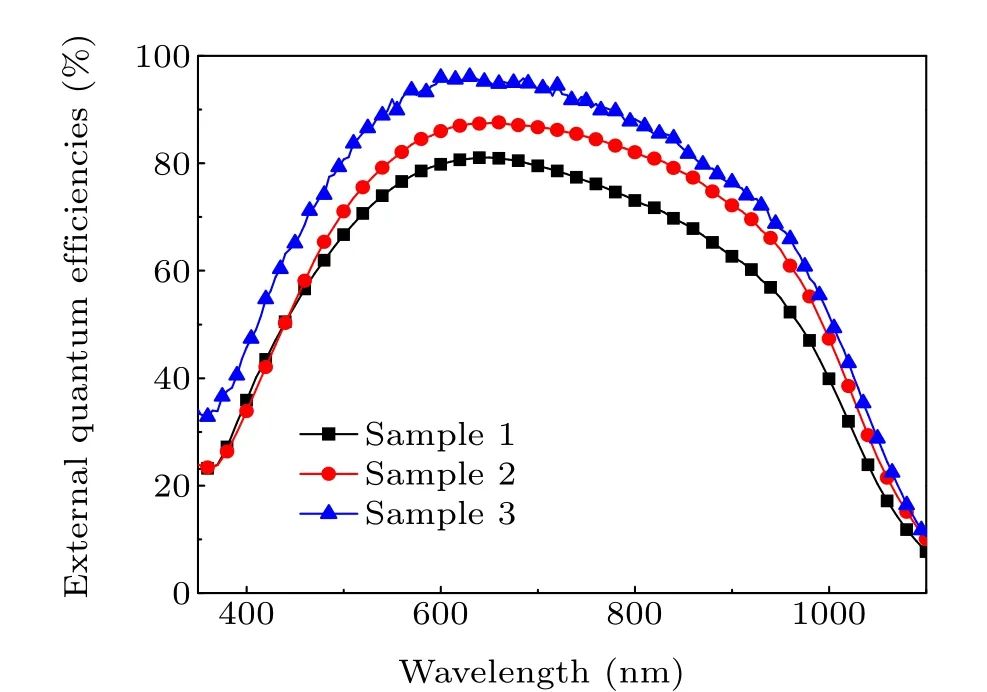
Fig.5. EQE spectra of samples 1-3.

Fig.6. The C-F curves of samples 1-3.
TheC-2-Vcurves of the three samples, as shown in Fig. 7, are measured at a frequency of 100 kHz. TheC-2-Vcurve of sample 1 is nonlinear, which indicates that the solar cell is not an abrupt junction. TheC-3-Vcurve, calculated from theC-Vdata, is also nonlinear, indicating that the solar cell is not a gradual junction. According to Eq. (1), for a single-sided junction, the impurity concentration (Nb) is obtained from the differential calculation of theC-Vcurve. The other two samples have abrupt junctions, as derived from the linear relationship of theC-2-Vcurves. According to Eq.(2),the built-in voltage(Vbi)of the p-n junction is obtained from the interception of the horizontal axis.[13]

TheVbivalues of samples 2 and 3 are 0.93 V and 0.72 V,respectively.Nbis calculated from the slope of theC-2-Vcurve. The values ofNband the depletion region width(W)atV=0 V are listed in Table 1, from which it can be observed that theNbof the three samples decreases,whileWgradually increases. The decrease inNbis consistent with the results of theC-Fcharacteristic measurements. This indicates that the introduction of the MoS2film and the p+layer reduces the impurity concentration of the solar cell. The increase inWis attributed to a decrease in the impurity concentration.The smaller value ofVbiand larger value ofVOCof sample 3,compared to those of sample 2,can be attributed to the partial voltage of the Schottky junction.
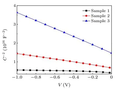
Fig.7. The C-2-V curves of samples 1-3.
4. Conclusion
In this study, the generation mechanism of the S-shapedJ-Vcurve was analyzed by introducing a MoS2film and a p+layer into the front and back surfaces of sample 1. The depletion region width was increased by the formation of a p-n junction,and a decrease in the impurity concentration was observed to reduce carrier recombination following the introduction of the MoS2film, which improved the photoelectric performance of the solar cell. A high-low junction was formed between the p+layer and the p-Si along with an ohmic contact between the p+layer and the Ag electrode because of the high doping characteristics and high work function of the p+layer.As a result,a higher current density output was obtained at a high voltage, and the S-shapedJ-Vcurve disappeared.Sample 3 was seen to exhibit ideal p-n junction rectification characteristics.The findings of this study may improve the application of MoS2thin films in the field of silicon-based solar cells,which are expected to be widely used in various siliconbased electronic and optical devices.
Acknowledgments
Project supported by the Science and Technology Research Project of Hebei Province Colleges and Universities(Grant No. QN2020113) and Tangshan Applied Basic Research Project(Grant No.19130227g).We would like to thank Editage(www.editage.cn)for English language editing.

- Chinese Physics B的其它文章
- Measurements of the 107Ag neutron capture cross sections with pulse height weighting technique at the CSNS Back-n facility
- Measuring Loschmidt echo via Floquet engineering in superconducting circuits
- Electronic structure and spin-orbit coupling in ternary transition metal chalcogenides Cu2TlX2(X =Se,Te)
- Characterization of the N-polar GaN film grown on C-plane sapphire and misoriented C-plane sapphire substrates by MOCVD
- Review on typical applications and computational optimizations based on semiclassical methods in strong-field physics
- Quantum partial least squares regression algorithm for multiple correlation problem