Effects of Strain Channel on Electron Irradiation Tolerance of InP-based HEMT Structures
2023-12-26 01:24FANGRenfengCAOWenyuWEIYanfengWANGYinCHENChuanliangYANJiashengXINGYanLIANGGuijieZHOUShuxing
原子能科学技术 2023年12期
FANG Renfeng, CAO Wenyu, WEI Yanfeng, WANG Yin, CHEN Chuanliang, YAN Jiasheng, XING Yan, LIANG Guijie,3, ZHOU Shuxing,3,*
(1.Hubei Key Laboratory of Low Dimensional Optoelectronic Materials and Devices, Hubei University of Arts and Science, Xiangyang 441053, China;2.Hubei Key Laboratory of High Power Semiconductor Technology, Hubei TECH Semiconductor Co., Ltd, Xiangyang 441021, China;3.Hubei Longzhong Laboratory, Xiangyang 441000, China)
Abstract: The introduction of strain InxGa1-xAs channel with high In content increases the confinement of the two-dimensional electron gas (2DEG) and further improves the high-frequency performance of InGaAs/InAlAs/InP HEMTs. The effect of InxGa1-xAs channel with different In contents on electron irradiation tolerance of InP-based HEMT structures in terms of 2DEG mobility and density has been investigated. The experiment results show that, after the same high electron irradiation dose, the 2DEG mobility and density in InP-based HEMT structures with strain InxGa1-xAs (x>0.53) channel decrease more dramatically than that without strain In0.53Ga0.47As channel. Moreover, the degradation of 2DEG mobility and density becomes more severe as the increase of In content and strain in the InxGa1-xAs channel. The research results can provide some suggestions for the design of radiation-resistant InP-based HEMTs.
Key words:InP-based HEMT; strain channel; two-dimensional electron gas; electron irradiation
In recent years, with the gradual maturation of terahertz technologies, indium phosphide based InGaAs/InAlAs high electron mobility transistors (InP-based HEMTs) have been intensively studied for their excellent high frequency, low noise figure, superior gain performance, and so on[1-4]. Indium phosphide based In0.53Ga0.47As/In0.52Al0.48As lattice-matched high electron mobility transistors (InP-based LM-HEMTs) exhibit outstanding performance due to the great electrical properties of In0.53Ga0.47As channel such as high saturation velocity and high electron mobility, but it is still subjected to short channel effects that hinder the improvement of high-frequency performance[5]. One solution is to use InP-based InxGa1-xAs/In0.52Al0.48As pseudomorphic high electron mobility transistors (InP-based PHEMTs) to provide better confinement for the wave function of two-dimensional electron gas (2DEG)[6-7]. The introduction of strain InxGa1-xAs (x>0.53) channel improves the 2DEG mobility and reduces short channel effects, which allows InP-based HEMTs to operate at a higher frequency. Due to the high frequency and low noise characteristics, InP-based HEMTs have excellent potential used for terahertz-wave transceiver communication system in deep-space exploration, satellite remote sensing and aerospace[8-10]. However, semiconductor devices and their integrated circuits operating in harsh space environments will be inevitably exposed to particles radiation, mostly electrons and protons, which will lead to performance deterioration of devices and even abnormality of electronic systems[11-13]. Therefore, the reliability of InP-based HEMTs integrated circuits in space remains an obstacle to the commercialization of large-scale space applications. For InP-based PHEMTs, strain InxGa1-xAs (x>0.53) channel brings better high-frequency performances to the devices, in the meantime inevitably affects the irradiation tolerance. But so far, to the best of our knowledge, there has not been a thorough analysis of the influence of strain InxGa1-xAs(x>0.53) channel on irradiation tolerance of InP-based HEMT structures.
In this work, we consider the effects of electron irradiation on the 2DEG mobility and density simultaneously and present a comprehensive analysis of the effects of electron irradiation on the performance of InP-based HEMT structures with and without strain channel. Electron irradiation on InP-based HEMT structures with different strain channels is carried out at various doses ranging from 2×10¹⁴to 1×1016cm-2. Further, the comparison of irradiation tolerance in InP-based HEMT structures with and without strain channel is demonstrated.
1 Experiment
All the epitaxial structures used in this experiment are provided by the Shanghai Institute of Microsystem and Information Technology, Chinese Academy of Sciences, which are grown by molecular beam epitaxy (MBE) system on semi-insulating InP substrates. Detailed growth details can be referenced from Refs. [7, 14]. The structure of InP-based HEMT is comprised of a semi-insulating InP substrate, a In0.52Al0.48As buffer layer with 300 nm thick, a strained InxGa1-xAs channel layer with 10 nm thick, a In0.52Al0.48As spacer layer with 3 nm thick, a 5×1012cm-2Si-δ-doped sheet layer, a In0.52Al0.48As barrier layer with 8 nm thick, a InP etching stopper layer with 4 nm thick, a n+-In0.52Al0.48As cap layer3 with 15 nm thick, a n+-In0.53Ga0.47As cap layer2 with 15 nm thick and a n+-In0.65Ga0.35As cap layer1 with 10 nm thick. In order to investigate the strain channel on electron irradiation tolerance of InP-based HEMT structures, epitaxial structures with channel In content of 0.53, 0.65, and 0.75 are prepared experimentally, which labeled as samples a, b, and c. When the In content is equal to 0.53, the strain is 0. As the In content increases, the strain increases. The hall data of the as-grown InP-based HEMT structures with different channel In contents are listed in Table 1.
The electron irradiation experiment is carried out at the Xinjiang Technical Institute of Physics and Chemistry, Chinese Academy of Sciences. All the epitaxial samples are vertically irradiated at room temperature (RT) using an ELV-8Ⅱ accelerator with 1.5 MeV electron beam at various doses ranging from 2×10¹⁴to 1×1016cm-2. Accordingly, the mobility (μ) and density (n) of 2DEG are measured by an Accent HL5500 Hall system at RT and 77 K as a function of irradiation dose, respectively.
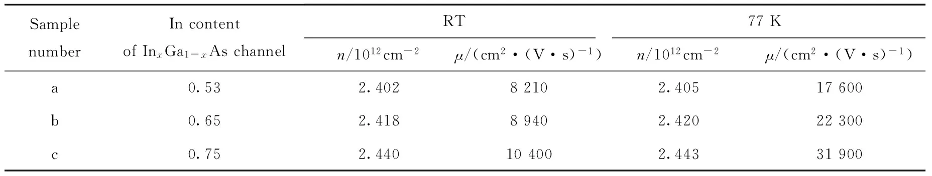
Table 1 Hall data of as-grown InP-based HEMT structures
2 Results
Fig.1 shows the dependence of 2DEG normalization mobility with electron irradiation dose measured at RT and 77 K, respectively. When the irradiation dose is lower than 2×1014cm-2, there is no obvious effect on the 2DEG mobility of the InP-based HEMT structures. As shown in Fig.1a, the decrease of 2DEG mobility is less than 2%. With the irradiation dose surpassing 2×1014cm-2, the 2DEG mobility begins to decrease obviously. A rapid downward trend is emerged at the irradiation dose ranging from 2×10¹⁴to 3×1015cm-2. Until the irradiation dose exceeds 3×1015cm-2, the 2DEG mobility decreases slowly and finally reaches saturation. Compared with Fig.1a and 1b, it is found that the degradation of 2DEG mobility at RT and 77 K exhibits a similar pattern. However, the degradation of 2DEG mobility at 77 K is even more serious than that at RT for samples irradiated at the dose ranging from 2×10¹⁴to 1×1016cm-2. As the In content of the InxGa1-xAs channel increases from 0.53 to 0.75, the degradation of 2DEG mobility in InP-based HEMT structures at RT and 77 K is becoming more severe at the same irradiation dose ranging from 2×10¹⁴to 1×1016cm-2. The experiment results show that the 2DEG mobility in InP-based HEMT structures with strain InxGa1-xAs (x>0.53) channel decreases more dramatically than that without strain In0.53Ga0.47As channel.
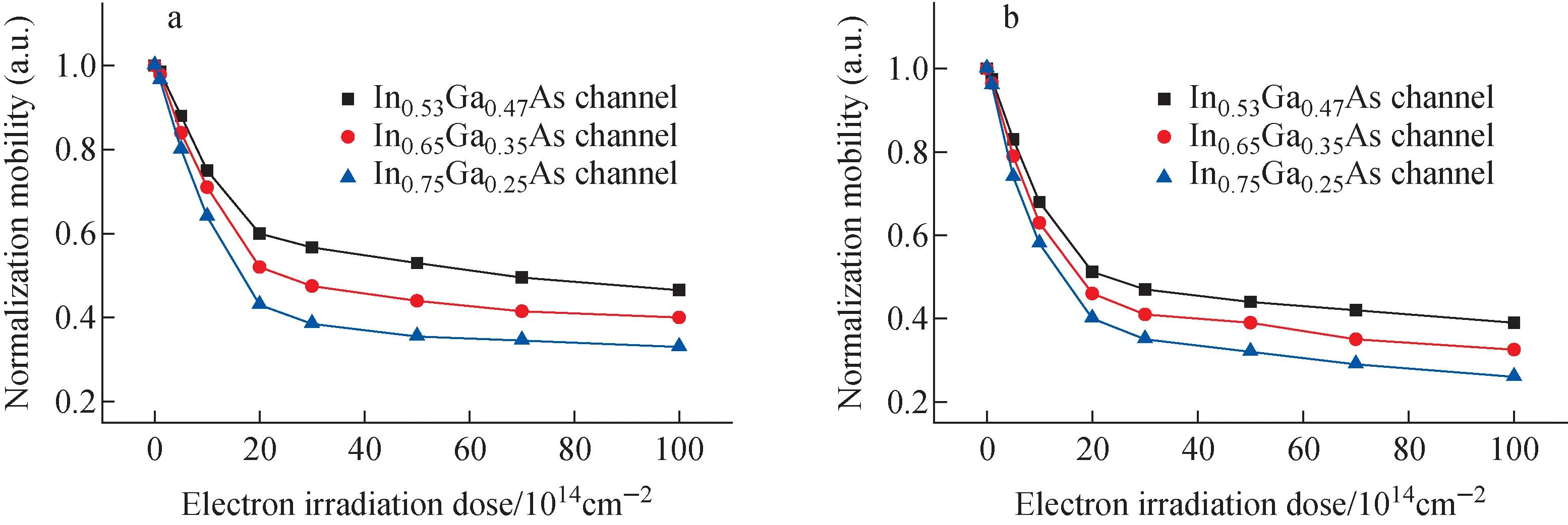
a—RT;b—77 KFig.1 Dependence of 2DEG normalization mobility with electron irradiation dose at different temperatures
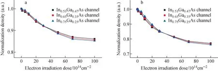
a—RT;b—77 KFig.2 Dependence of 2DEG normalization density with electron irradiation dose at different temperatures
Fig.2 shows the dependence of 2DEG normalization density with electron irradiation dose measured at RT and 77 K, respectively. When the irradiation dose is lower than 2×1014cm-2, there is no obvious effect on the 2DEG density of the InP-based HEMT structures, as shown in Fig.2a. After the electron irradiation dose exceeds 2×1014cm-2, the 2DEG density starts to decrease slowly at the dose ranging from 2×10¹⁴to 5×1014cm-2. Once the irradiation dose exceeding 5×1014cm-2, the 2DEG density begins to decline rapidly. A rapid downward trend is emerged at the irradiation dose ranging from 5×10¹⁴to 7×1015cm-2. Until the irradiation dose surpassing 7×1015cm-2, the 2DEG density decreases slowly and finally reaches saturation. Compared with Fig.2a and 2b, it is found that the degradation of 2DEG density at RT and 77 K exhibits a similar pattern. However, the decrease of 2DEG density at 77 K is more serious than that at RT for samples irradiated at the dose ranging from 2×10¹⁴to 1×1016cm-2. As the In content of the InxGa1-xAs channel increases from 0.53 to 0.75, the degradation of 2DEG density in InP-based HEMT structures at RT and 77 K weakens at the same irradiation dose ranging from 2×10¹⁴to 3×1015cm-2. After the irradiation dose exceeding 3×1015cm-2, it can be observed that the degradation of 2DEG density in InP-based HEMT structures becomes more severely with the increase of the In content of the InxGa1-xAs channel. The experiment results also show that the 2DEG density in InP-based HEMT structures with strain InxGa1-xAs (x>0.53) channel decreases more dramatically than that without strain In0.53Ga0.47As channel.
3 Discussions
The 2DEG of InP-based HEMT epitaxial materials comes from InGaAs/InAlAs quantum wells, and its transport characteristics are mainly influenced by the energy band structure of InGaAs/InAlAs heterostructures and various scattering processes such as ionization impurity scattering, Coulomb scattering, alloy scattering[7]. Commonly, in order to enhance the transport characteristics of the 2DEG, the strain InxGa1-xAs (x>0.53) channel will be applied to the InP-based HEMT epitaxial structures. During the growth of strain InxGa1-xAs/InAlAs quantum well channel, the symmetry of the lattice changes due to the introduction of strain layers. The lateral lattice of the epitaxial layer undergoes compressive strain, causing the lateral lattice constant to match the substrate. This means that the lattice in two directions parallel to the InGaAs/InAlAs heterojunction plane will shrink relatively and be subjected to biaxial compressive stress, while the longitudinal lattice will elongate and undergo tensile strain. In the biaxial compressive strain layer, the net bandgap shift[15]is:
ΔE=-α·ε≥0
(1)
whereαis the deformation potential, which is related to the elastic constant of the material and is greater than 0,εis the compressive strain, which is less than or equal to 0. From the above formula, it can be seen that the increase ofεwill lead to the increase of ΔEfor the heterojunction. If theεdisappears, the movement of ΔEwill also disappear. As the In content of the InxGa1-xAs channel increases, theεwill correspondingly increase. Then the potential well of InGaAs/InAlAs quantum well channels will become deeper with the increase of In content to provide better confinement for the wave function of 2DEG. Consequently, the scattering on 2DEG in the quantum well is much reduced and the 2DEG mobility rapidly increases. At the same time, the electrons of ionizing donor impurity are more easily transferred to the quantum well, resulting in a slight increase of 2DEG density in the quantum well, as shown in Table 1.
When InP-based HEMT epitaxial structures are irradiated by high energy electron beam, electrons will interact with lattice atoms in the material, resulting in elastic collisions or inelastic collisions. The collided lattice atoms will gain enough energy to overcome the binding of surrounding atoms and squeeze into the lattice gaps. At the same time, the original lattice position becomes a vacancy. The process leads to the formation of radiation-induced point defect[16]. Generally, after electron irradiation, high energy electron irradiation can lead to radiation-induced defects such as point defects, alloy disorder, as well as remote ionization impurity migration in the channel heterojunction region of InGaAs/InAlAs quantum well, which will disrupt the periodicity of the lattice and generate localized defect energy levels in the lattice bandgap of the quantum well region. After the irradiation dose surpassing 2×1014cm-2, the scattering resulting from radiation-induced point defects, alloy disorder, as well as remote ionization impurity migration on 2DEG in the channel quantum well will be enhanced, which will result in an obvious decrease of 2DEG mobility in InP-based HEMT epitaxial structures, as is shown in Fig.1. In addition, some of the radiation-induced defect energy levels will become carrier capture centers. After capturing charge carriers, the formation of additional charge will weaken the built-in electric field at the InGaAs/InAlAs heterojunction interface in the channel quantum well, reduce the degree of energy band bending, and make the triangular potential well at the heterojunction interface shallower[16], resulting in a decrease of 2DEG density, as shown in Fig.2. This phenomenon has been reported in InP-based HEMT epitaxial structures irradiated by electrons[17].
After electron irradiation dose exceeds a certain value, the introduction of radiation-induced defects will lead to strain relaxation in partially mismatched strain lattices, resulting in the lattice constant of the strain InGaAs channel layer no longer being equal to the lattice constant of InP substrate. Strain energy is released by generating dislocation defects in the heterojunction interface of InGaAs/InAlAs quantum well. Compared to the InP-based lattice-matched HEMT, the heterojunction interface of InGaAs/InAlAs quantum well in the InP-based PHEMT generates more radiation-induced defects originating from strain relaxation after electron irradiation dose exceeding a certain value. Moreover, the greater the strain in the channel, the more radiation-induced defects will be released at channel heterojunction interface. Thus, the degradation of 2DEG mobility in InP-based HEMT epitaxial structures at RT and 77 K is becoming more severe at the same irradiation dose ranging from 2×10¹⁴to 1×1016cm-2as the In content of the InxGa1-xAs channel increases from 0.53 to 0.75, as shown in Fig.1. At the same time, the decrease of compressive strain resulting from strain relaxation will lead to the reduction of net conduction band gap for the InGaAs/InAlAs heterojunction interface in the quantum well. As a result, the triangular potential well will further become shallower and the curvature of the energy band will be much reduced[18]. As a consequence, the confinement for the wave function of 2DEG will be significantly weakened, which result that the scattering coming from radiation-induced point defect, alloy disorder, remote ionization impurity migration on the 2DEG will be significantly enhanced and the 2DEG density will be further reduced. So, the degradation of 2DEG density in InP-based HEMT epitaxial structures becomes more severely with the In content increase in the InxGa1-xAs channel, after the irradiation dose exceeding 3×1015cm-2, as is shown in Fig.2.
4 Conclusions
In summary, the effect of electron irradiation on InP-based HEMT epitaxial structures with different strain channels is systematically investigated by considering the impact of electron irradiation on 2DEG mobility and density. Our experiment results show that the degradation of 2DEG mobility and density at RT and 77 K becomes more severe as the increase of In content and strain in the InxGa1-xAs channel after the same high electron irradiation dose. The experiment results also demonstrate that the 2DEG mobility and density at RT and 77 K in InP-based HEMT epitaxial structures with strain InxGa1-xAs (x>0.53) channel decrease more dramatically than that without strain In0.53Ga0.47As channel, which indicates the InP-based LM-HEMT epitaxial structures may have a better electron irradiation tolerance than the InP-based PHEMT epitaxial structures. It can be attributed to that the introduction of radiation-induced defects in the InP-based PHEMT epitaxial structures will lead to more dislocation defects and reduction of net conduction band gap duo to strain relaxation in the heterojunction interface of strain InxGa1-xAs (x>0.53) channel quantum well, compared to the InP-based LM-HEMT epitaxial structures. The results may give some suggestions to those designing of the radiation-resistant InP-based HEMTs.