Design of Novel and Low Cost Triple-node Upset Self-recoverable Latch
2023-12-26 01:03BAINaMINGTianboXUYaohuaWANGYiLIYunfeiLILi
原子能科学技术 2023年12期
BAI Na, MING Tianbo, XU Yaohua, WANG Yi,3, LI Yunfei,3, LI Li
(1.Information Materials and Intelligent Sensing Laboratory of Anhui Province, Anhui University, Hefei 230601, China; 2.Shanxi Key Laboratory of Advanced Semiconductor Optoelectronic Devices and Integrated Systems, Jincheng 048000, China;3.Jincheng Research Institute of Opo-mechatronics Industry, Jincheng 048000, China)
Abstract: With the development of semiconductor technology, the size of transistors continues to shrink. In complex radiation environments in aerospace and other fields, small-sized circuits are more prone to soft error (SE). Currently, single-node upset (SNU), double-node upset (DNU) and triple-node upset (TNU) caused by SE are relatively common. TNU’s solution is not yet fully mature. A novel and low-cost TNU self-recoverable latch (named NLCTNURL) was designed which is resistant to harsh radiation effects. When analyzing circuit resiliency, a double-exponential current source is used to simulate the flipping behavior of a node’s stored value when an error occurs. Simulation results show that the latch has full TNU self-recovery. A comparative analysis was conducted on seven latches related to TNU. Besides, a comprehensive index combining delay, power, area and self-recovery—DPAN index was proposed, and all eight types of latches from the perspectives of delay, power, area, and DPAN index were analyzed and compared. The simulation results show that compared with the latches LCTNURL and TNURL which can also achieve TNU self-recoverable, NLCTNURL is reduced by 68.23% and 57.46% respectively from the perspective of delay. From the perspective of power, NLCTNURL is reduced by 72.84% and 74.19%, respectively. From the area perspective, NLCTNURL is reduced by about 28.57% and 53.13%, respectively. From the DPAN index perspective, NLCTNURL is reduced by about 93.12% and 97.31%. The simulation results show that the delay and power stability of the circuit are very high no matter in different temperatures or operating voltages.
Key words:circuit reliability; latch design; self-recoverability; soft error; radiation hardening; triple-node upset
The level of integration and performance of integrated circuits (ICs) and systems increase with the dramatic reduction in transistor feature size. However, the susceptibility of CMOS integrated circuits and systems to soft errors (SEs) seriously increase, especially in harsh radiation environments. SEs are caused by impacts of alpha particles, heavy ions, neutrons, etc.[1]. SEs occur when high-energy particles strike sensitive areas of a transistor and create electron-hole pairs (EHP)[2]. Consequently, transistors in the OFF state begin to conduct temporarily and change the logic level of the affected node. Therefore, a glitch is generated on the node, which will lead to a transient fault (TF) and possibly a system failure or SE[3]. Furthermore, energetic particles may affect multiple nodes due to the reduction of node capacitance and inter-node spacing. SEs include single-node upset (SNU)[4]and multi-node upset (MNU)[5]. MNU includes double-node upset (DNU) and triple-node upset (TNU). MNU will seriously affect the reliability of IC and system in harsh radiation environment[6].
In the combinatorial logic circuits, even if the node is disturbed by the particle incident, when the upset is over, the combinatorial logic circuits can restore the original level, so in most applications, the SE of the combinatorial logic circuits is not considered. In sequential logic circuits and storage circuits, due to the existence of feedback signals, if a SE occurs at a node, the circuit may latch the error level signal after the soft error occurs at the node through the feedback path. SEs are more sensitive[7]. As a key unit in sequential logic circuits, latches are important to improve their resistance to SEs[7-9].
Radiation hardening by design (RHD) is the most effective technique to tolerate SEs caused by energetic particles. Over the past decade, there was extensive research in the field of radiation-hardened memory cells (latches/flip-flops) for soft-error-induced multi-node upsets.
In this paper, the circuit redundancy design, clock gating, and high-speed transmission technology will be used to design a new latch. The latch is composed of an interlocked input separation inverter (IINV), which forms two feedback loops when storing different information to achieve complete TNU self recovery function. The use of fewer transistors and symmetrical structures makes the latch have good delay and power consumption characteristics, and the robustness of the latch to single event events will be verified through simulation technology in 28 nm CMOS.
1 Latch design
1.1 Existing latches
Most of the existing radiation-resistant latches can only achieve SNU self-recovery[10,13-16]. Only a few can achieve TNU self-recovery[5-6]. TNUCT[10]mainly consists of a two-input C-element[11]and DICE[12]based on quadruple cross-coupled clock gating, which has high power characteristics. TNUHL[13]output stage circuit consists of two three-input and one two-input C-element, its delay is larger than other latches. The delay and power of TNUHLPro[14]are relatively high. The main idea of LCTNUT[15]is to intercept errors, and its delay and power are very low, and the overall performance is excellent. TNUTL[16]consists of five input-split C-element and a two-input-element, forming the main latch unit. Its characteristics are smaller area, higher delay and lower power. LCTNURL[5]consists of 12 three-input C-elements. In order to realize the complete self-recovery of TNU, the silicon chip area is increased. TNURL[6]can automatically restore to the correct logic value in a short time. However, its structure is relatively complex to implement, and both area and power are very expensive.
In order to solve the above mentioned problems, a new type of latch is designed, which has the same TNU self-recovery capability as LCTNURL and TNURL, and lower delay, power consumption and area than the previous two latches.
1.2 NLCNTURL
The latch designed in this paper named NLCNTURL is shown in Fig.1a, which is composed of an input unit, an output unit and two self-restoring (RC) units.
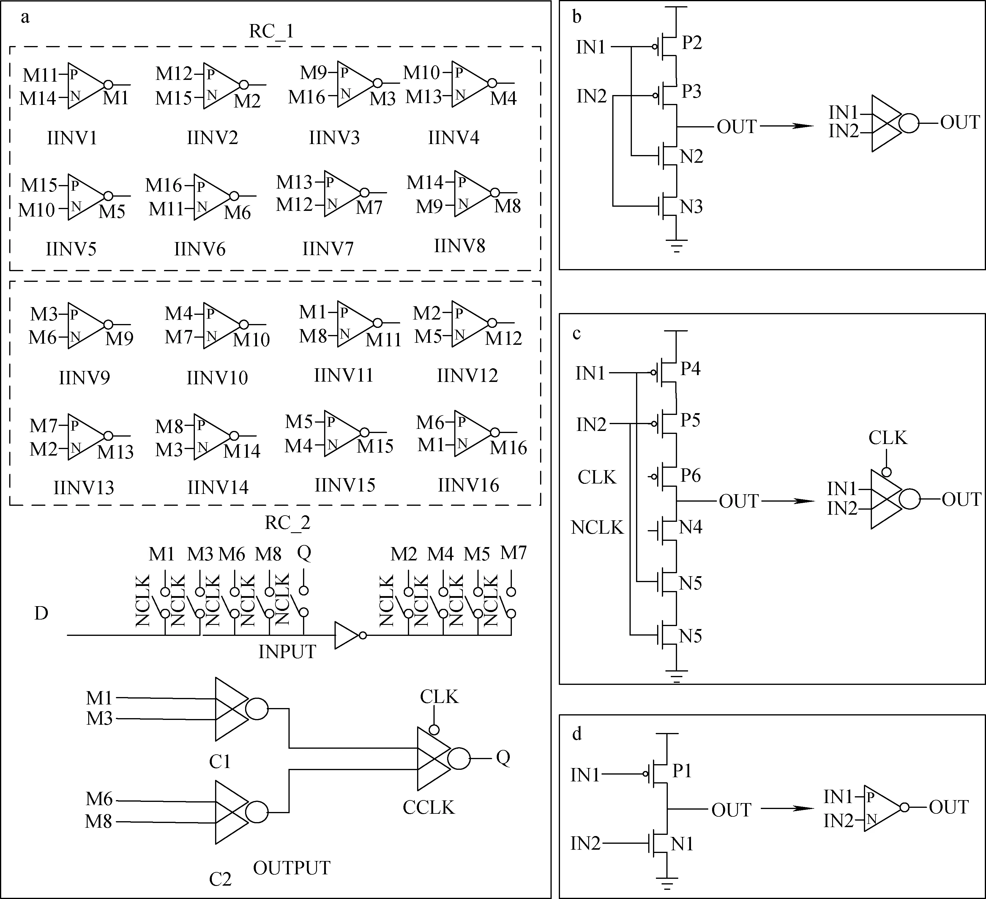
Fig.1 Schematic of NLCNTURL (a), C-element (b), C-element with clock (c), and IINV (d)
The input unit directly connects the input signal to be stored from the input node D to the output node Q through the TG, thereby realizing high-speed transmission. D will also precharge 8 nodes of the RC unit through 8 TGs. M1, M3, M6, M8 have the same level information as D, so they are called positive input (PI) nodes, M2, M4, M5, M7 have the opposite level information to D and therefore are called reverse input (RI) node. The output unit first inputs the value of the PI node into two two-input C-element respectively (Fig.1b), and then connects its output to the two-input C-element with clock as shown in Fig.1c to prevent current contention and reduce power. The RC unit consists of 16 IINVs (Fig.1d). Due to its special structure and redundant information storage characteristics, the nodes that are precharged by IINV through PI nodes are defined as reverse redun-dant (RR) nodes, including M9, M11, M14,and M16. The nodes whose RI nodes are precharged by IINV are defined as positive redundant (PR) nodes, including M10, M12, M13, and M15.
In this paper, the term CLK is defined as the normal clock signal, while NCLK means the inverted signal of CLK. When CLK=0, NCLK=1, the system is in transparent mode, and the input signal directly affects the output through the TG. TakingD=0 as an example, the input signal is first transmitted to the input node through the TG, so thatM1=M3=M6=M8=0,M2=M4=M5=M7=1, and then in RC_2, the PI group nodes sequentially transmit the signal to M11, M9, M16, M14 through IINV11, IINV9, IINV16, IINV14. RI group nodes sequentially transmit the signal to M13, M15, M12, M10 through IINV13, IINV15, IINV12, IINV10, and finally form the feedback loops, as shown in Fig.2a and Fig.2b. The feedback loop whenD=1 is shown in Fig.2c and Fig.2d.
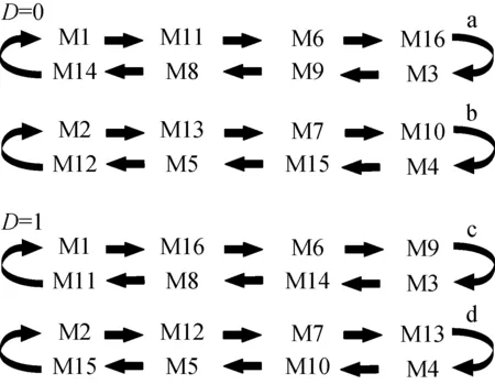
Fig.2 Schematic of feedback loop
When CLK=1, NCLK=0, the system is in latch mode, at this time the TGs are closed, and the output value is determined by the latch signal of the RC unit passing through the output unit. When this state system generates SEs, it is possible to cause output errors, so the fault-tolerant analysis of the system in this paper is based on this state.
2 Functional simulation
2.1 Normal operation
The NLCNTURL was simulated in SPICE with models derived from a 28-nm technology. The lengths of the transmission-gate transistors were set atL=30 nm, with PMOS widths set toW=200 nm and NMOS widths set toW=100 nm. The simulated results for normal operation with a clock frequency of 100 MHz and an operating voltage of 1.2 V is shown in Fig.3.

Fig.3 Simulated waveforms of CLK, D, Q of NLCTNURL under normal working condition
2.2 SNU/DNU/TNU recovery analysis
AssumingD=0, thenM1=M3=M6=M8=M10=M12=M13=M15=0,M2=M4=M5=M7=M9=M11=M14=M16=1, and the corresponding feedback loops are shown in Fig.2a and Fig.2b. Fault injection is modeled using a double exponential current source model. The equations for the injection current source and the accumulated charge are presented as follows:
(1)
Io=Q/(τα-τβ)
(2)
Where,Iois an approximation of the peak current,ταrepresents the collection time constant of the junction,τβrepresents the time constant of the initial ion trajectory establishment, andQis the total deposited charge.
To facilitate the calculation,ταis set to 200 ps, andτβis set to 50 ps in this experiment.
1) SNU
When SNU appears in the system, it can be divided into two main situations: the input node of all IINV (Case 1) and the output node Q (Case 2). The simulation waveform of SNU self-recoverable is shown in Fig.4. All parts marked with red lightning in Fig.4 are simulated fault injections. As can be seen from Fig.4, all nodes can return to their original states after being flipped. The statistic results for the complete key SNU latch design according to Fig.4 is listed in Table 1.
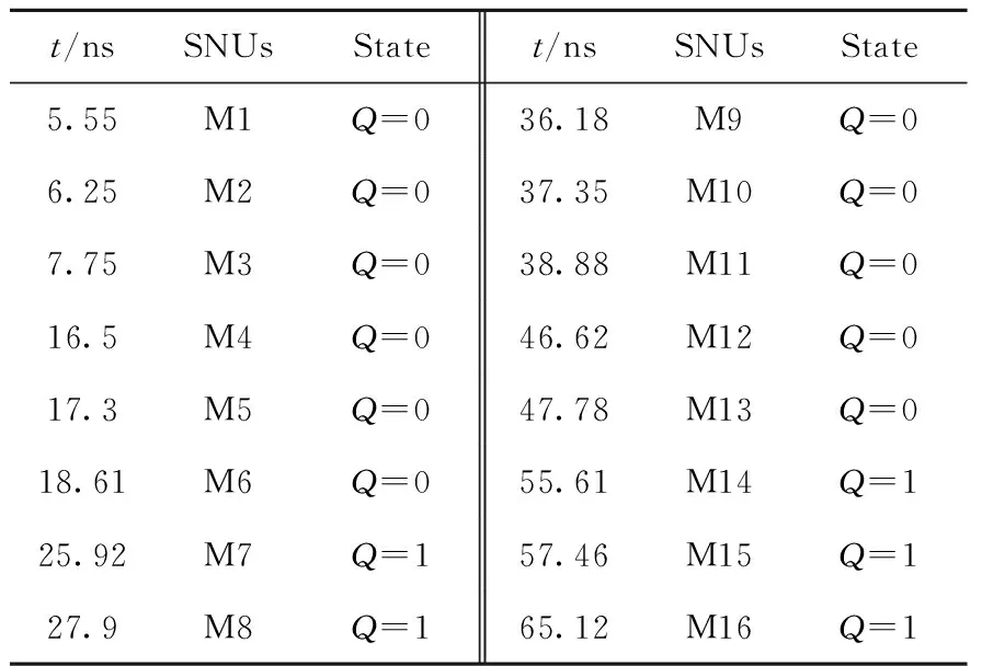
Table 1 Statistic results for complete key SNU latch design according to Fig.4
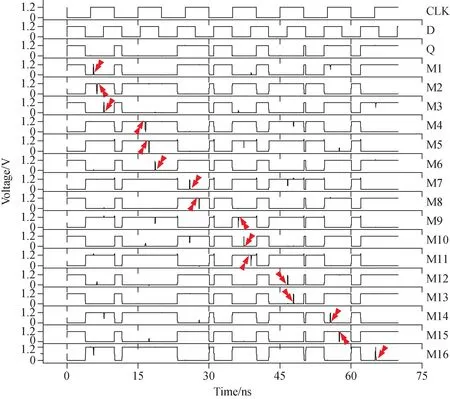
Fig.4 Simulated waveform of SNU self-recoverable
For the Case 1, take M1 flipping from 0 to 1 as an example, as shown at 5.55 ns in Fig.4. At this time, there are IINV11 and IINV16 that take M1 as input. First analyze IINV11, because the original state of M1 and M8 is 0, the PMOS in IINV11 is turned on, and the NMOS is turned off. At this time, the flip of M1 will cause the PMOS to be turned off, the output of M11 node is in a high-impedance state, and the information does not change. Then analyze IINV16, because the original state of M6 is also 0 (strong 0), at this time M1 is flipped from 0 to 1 (weak 1), which is not enough to affect the output of M16, so the information does not change. From these it can be concluded that if one of the two inputs to IINV is flipped independently, the error will not be propagated down. At this time, the values of the two inputs M11 and M14 of IINV1 with M1 as the output don’t change, so the value of M1 can be recovered.
For the Case 2, When Q flips, because Q is not fed back to any node, the nodes in the RC unit still store the correct value, and the PI node will restore the value of Q through the output unit.
2) DNU
When DNU occurs in the system, it is mainly divided into three situations: the input node of different IINV (Case 1), two input nodes of the same IINV (Case 2), the input node of IINV and the output on the node (Case 3). The DNU self-recovery simulation waveform is shown in Fig.5. Fig.5 shows that two red lightning bolts occur on different nodes at the same time, indicating that the two nodes have flipped, and all the nodes that have flipped can restore their original values. The statistic results for the complete key DNU latch design according to Fig.5 is listed in Table 2.
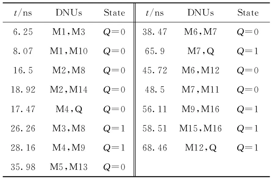
Table 2 Statistic results for complete key DNU latch design according to Fig.5

Fig.5 Waveform diagram of simulation result of DNU self-recoverable
For the Case 1, take {M1, M3} flipping from 0 to 1 as an example, as shown at 6.25 ns in Fig.5. At this time, the input flipped are IINV9, IINV11, IINV14, and IINV16. From the Case 1 in SNU, it can be seen that the error will not be passed down, and other nodes will not be affected. It can be seen from the feedback loop that M1 can be restored by M14 through IINV1, and M3 can be restored by M16 through IINV3.
For the Case 2, take {M3, M8} flipping from 0 to 1 as an example (the output at 26.26 ns in Fig.5 is the output whenQ=1, just for reference). At this time, the two inputs of IINV14 are all inverted, so the value of M14 is also inverted from 1 to 0. There are IINV1, IINV8, IINV9, and IINV11 with a single input flip. These errors will not be passed down, so only the three nodes of M3, M8, and M14 are flipped. It can be seen from the feedback loop that M3 can be recovered by M16 through IINV3, and M8 can be recovered by M16. M9 is restored by IINV8, and finally M14 is restored by M8 by IINV14.
For the Case 3, take the {M4, Q} flip as an example, as shown at 17.47 ns in Fig.5. From the analysis of SNU, it can be known that M4 acts as a single flipped IINV input node, and the error will not be passed down. Q will not be fed back to other nodes, nor will it affect other nodes. There is a feedback loop, M4 can be recovered by M10 through IINV4, and Q can be recovered by the output unit.
3) TNU
When TNU occurs in the system, it can be mainly divided into four situations: flipping occurring on inputs of different IINV, two flips occurring on the input of one IINV and the other on the other IINV input, exactly three flips causing the inputs of both IINVs to flip, the inversion occurring between the RC unit and the output node Q.
The simulated waveform diagram is shown in Fig.6, and the statistic results for complete key TNU latch design according to Fig.6 is listed in Table 3.
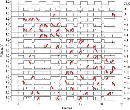
Fig.6 Simulated waveform of TNU self-recoverable
(1) Flipping occurs on inputs of different IINV. Take {M1, M3, M13} flipping from 0 to 1 as an example, as shown at 5.71 ns in Fig.6. At this time, IINV4, IINV7, IINV9, IINV11, IINV14, and IINV16 are all independent inputs and flipped. According to the analysis of SNU, errors will not be passed down. It can be seen from the feedback loop that M1 can be restored by M14 through IINV1, M3 can be restored by M16 through IINV3, and M13 can be restored by M2 through IINV13.
Table 3 Statistic results for complete key TNU latch design according to Fig.6
(2) Two flips occur on the input of one IINV and the other on the other IINV input. Take the flipping of {M1, M8, M9} as an example, as shown at 7.12 ns in Fig.6. At this time, M1 and M8 are flipped at the same time, causing the result of IINV11 to be wrong, and M11 is flipped from 1 to 0. However, IINV1, IINV3, IINV6, IINV8, IINV14, and IINV16 are all independent input flips, and the error will not be passed down. It can be seen from the feedback loop that M1 can be restored by M14 through IINV1, M9 can be restored by M3 through IINV9, then M8 can be restored by M9 through IINV8, and M11 can be restored by M1 through IINV11.
(3) Exactly three flips cause the inputs of both IINVs to flip. Take {M12, M13, M15} flip as an example. At this time, the inputs of IINV2 and IINV7 are all inverted, causing the values of M2 and M7 to also be inverted, thus causing the two inputs of IINV13 to also be inverted. Others are independent input flips, and have no effect on other nodes. From the feedback loop, M15 can be recovered by M4, M12 can be recovered by M5, M2 can be recovered by M12, M13 can be recovered by M2, and M7 can be recovered by M13.
(4) The inversion occurs between the RC unit and the output node Q. It can be seen that the Case 1 or Case 2 in DNU occurs in the RC unit and the output node Q is inverted. Since the DNUs in the RC unit can be self-recovery, the change of the output node Q will not affect any node, so Q can finally recover its own value through the correct value recovered by the RC unit.
3 Overheads
The area, DPAN, delay, and power of the NLCNTURL are shown in Fig.7, the experiments condition is 28 nm process, 27 ℃, and 1.2 V. In which, area refers to the silicon area calculated using formula (3), DPAN represents the product of delay, power and silicon area required for each self-recovery node, as shown in formula (4). Delay, power and area are multiplied and then divided by the number of nodes and the latch can self-recover. DPAN can be used to comprehensively analyze the performance of the latch.
(3)
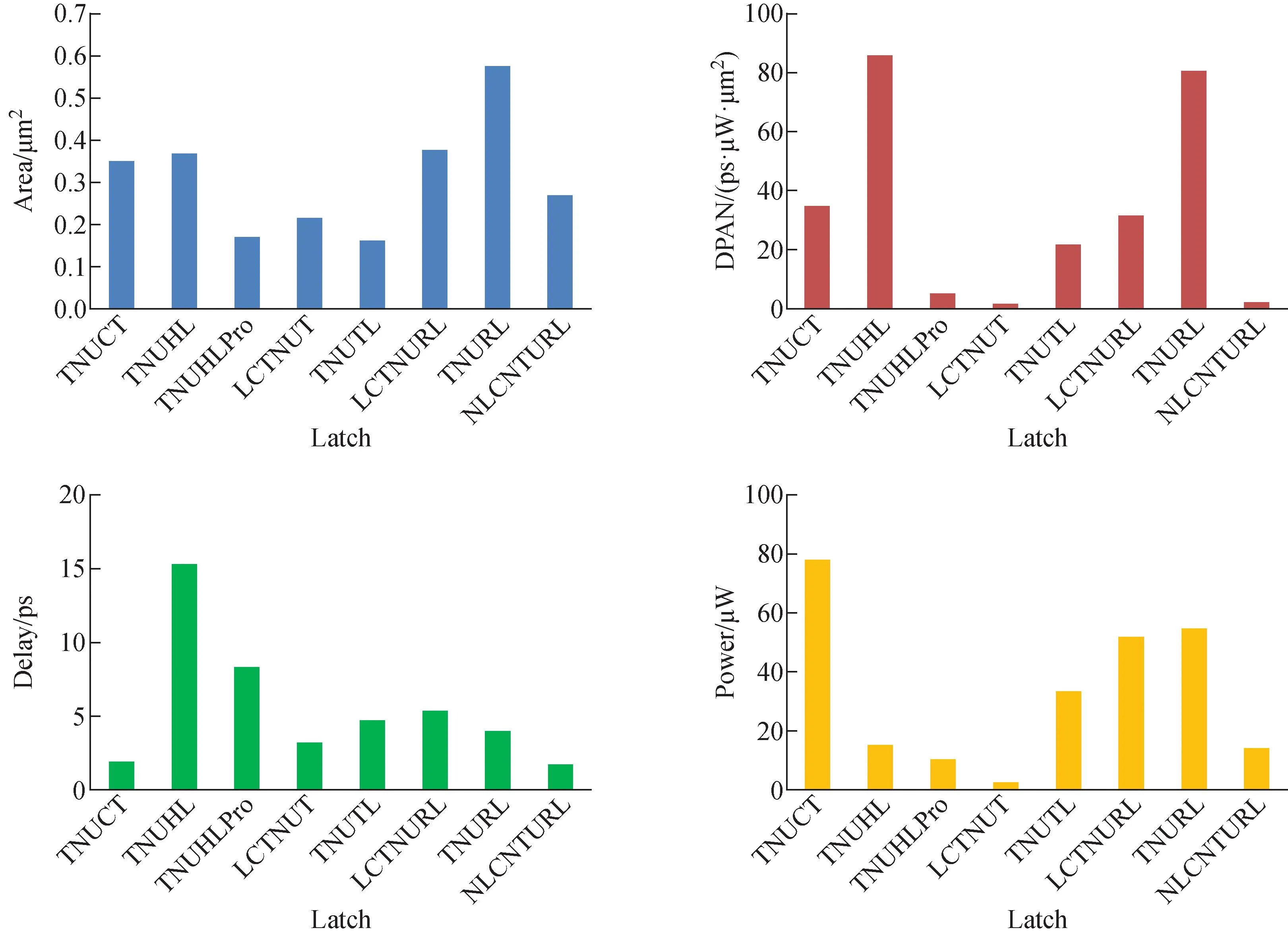
Fig.7 Comparison of area, DPAN, delay and power of different latches
(4)
Where,n1is the number of nMOS,LnMOS(i) andWnMOS(i) are the effective length and width of each nMOS, respectively,n2is the number of pMOS,LpMOS(i) andWpMOS(i) are the effective length and width of each pMOS, respectively. Node refers to the number of latch nodes capable of self-recovery. For example, NLCNTURL can self-recover TNU, then Node=3. Power refers to the average power per cycle, and delay refers to the propagation delay from D to Q, which is the average of the rise and fall delays from D to Q.
As shown in Fig.7, NLCNTURL completes a complete TNU self-recoverable function without increasing a lot of area, only 0.27 μm2. Compared with TNUTL, the area only increases by 40%, and TNUTL cannot provide TNU self-recoverable function. Compared with LCTNURL and TNURL, which can also provide TNU self-recoverable function, the area reduces by 28.57% and 53.13%, respectively. As for the DPAN, which represents the comprehensive performance, the performance of NLCNTURL is much better than that of other latches except LCTNUT, with only 2.169 ps·μW·μm2.
Since the circuit uses a fast switching device, the total capacitance is small, the transistors of the latch unit are less, the path experienced by the transmission process is shorter, and the aspect ratio of the transistors used by the key latch unit is set smaller, so the average delay and power required by the latches are controlled. Delay is even the smallest among all latches, with an average delay of only 1.706 ps at room temperature and 1.2 V. On the contrary, TNUHL with the largest delay does not use clock gating technology, the input is not directly connected to the output, and the stability and synchronization of each part of the circuit cannot be guaranteed, so the delay time of the circuit is longer. The power is relatively small, because multiple transmission gates are added, and the delay is optimal when a small power is added. And it is 72.84% smaller than LCTNURL, and 74.19% smaller than TNURL.
Another parameters which should be considered when evaluating the performance of latch are voltage and temperature.
The impact of power supply voltage (1-1.4 V) on power and delay is shown in Fig.8a and Fig.8b. When the supply voltage increases, the delay of the latch decreases and the power increases. The reason is that by increasing the supply voltage, the dynamic and static power increases (the capacitor accumulates more charge and the transistor drives more current[17]). A large supply voltage can reduce the delay of the transistor, but will increase the power. Since the fast switch can respond to voltage changes within nanoseconds, the response time of the circuit is greatly shortened. When the voltage of NLCTNURL changes by 0.4 V, the delay only changes by 0.507 ps. However, although the high-speed transmission technology is used, more TGs are used, which makes the power less stable under the condition of voltage changes.
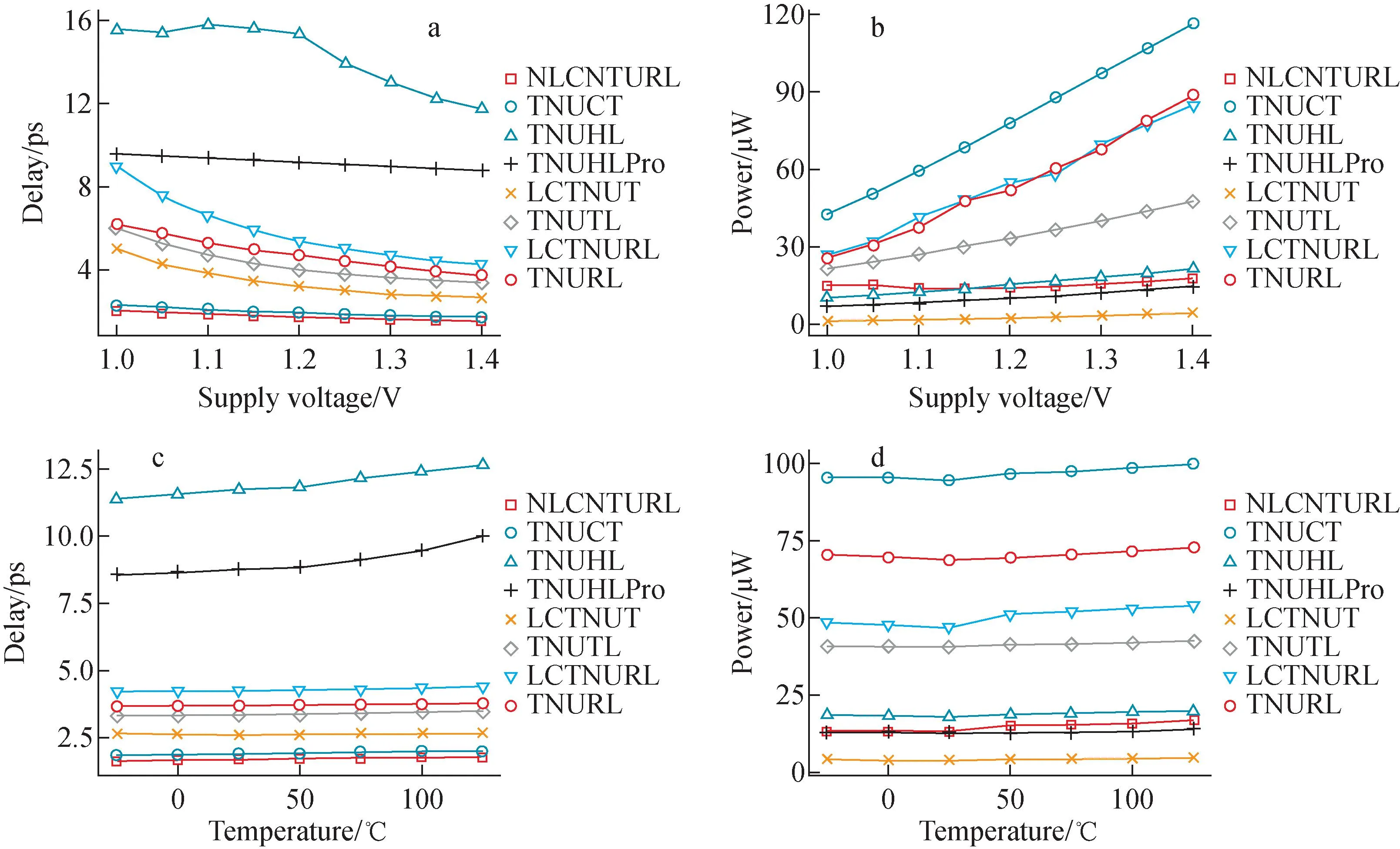
Fig.8 Voltage and temperature fluctuation analysis results
In real IC applications, temperatures can vary significantly from cold startup moments to hot periods of operation. From process considerations, the actual situation was simulated within the temperature range of -25 ℃ to 125 ℃ in this paper, and the performance of the latch was observed at different temperatures. As shown in Fig.8d, the performance of the latch is the best when it is close to room temperature. At high and low temperatures, the performance of the latch will decrease. The effect of temperature on power and delay (D-Q) is shown in Fig.8c and Fig.8d. As the temperature increases, the latency and power consumption of locked memories generally increase, mainly because the carrier mobility decreases when the temperature increases[11], but since the transistors used have good temperature stability and there are no temperature sensitive devices, so the above-mentioned latches have good temperature stability, especially in NLCNTURL. When the temperature changes by 150 ℃, the delay only changes by 0.137 ps and the power only changes by 3.9 μW.
4 Conclusion
In order to reduce TNU errors caused by SEs generated by storage cells in complex radiation environment, NLCTNURL was designed in this paper. The latch is composed of interlocked IINV, which form two feedback loops when storing different information. The output of the IINV in the latch is always fed back to the input of the other IINV to provide the full TNU self-recoverable feature. And due to the use of fewer transistors and a symmetrical structure, compared with LCTNURL, NLCNTURL reduces delay by 68.34%, power by 72.84%, and DPAN by 93.12%. Compared with TNURL, the delay reduces by 63.98%, the power reduces by 74.19%, and the DPAN reduces by 97.31%.