Laser-assisted Simulation of Dose Rate Effects of Wide Band Gap Semiconductor Devices
2023-12-26 01:24TANGGeXIAOYaoSUNPengLIUJingruiZHANGFuwangLIMo
原子能科学技术 2023年12期
TANG Ge, XIAO Yao, SUN Peng, LIU Jingrui, ZHANG Fuwang, LI Mo
(1.Chengdu University of Technology, Chengdu 610059, China;2.University of Electronic Science and Technology of China, Chengdu 610054, China;3.Microsystem &Terahertz Research Center of CAEP, Chengdu 621000, China)
Abstract: Laser-assisted simulation technique has played a crucial role in the investigation of dose rate effects of silicon-based devices and integrated circuits, due to its exceptional advantages in terms of flexibility, safety, convenience, and precision. In recent years, wide band gap materials, known for their strong bonding and high ionization energy, have gained increasing attention from researchers and hold significant promise for extensive applications in specialized environments. Consequently, there is a growing need for comprehensive research on the dose rate effects of wide band gap materials. In response to this need, the use of laser-assisted simulation technology has emerged as a promising approach, offering an effective means to assess the efficacy of investigating these materials and devices. This paper focused on investigating the feasibility of laser-assisted simulation to study the dose rate effects of wide band gap semiconductor devices. Theoretical conversion factors for laser-assisted simulation of dose rate effects of GaN-based and SiC-based devices were been provided. Moreover, to validate the accuracy of the conversion factors, pulsed laser and dose rate experiments were conducted on GaN-based and SiC-based PIN diodes. The results demonstrate that pulsed laser radiation and γ-ray radiation can produce highly similar photocurrent responses in GaN-based and SiC-based PIN diodes, with correlation coefficients of 0.98 and 0.974, respectively. This finding reaffirms the effectiveness of laser-assisted simulation technology, making it a valuable complement in studying the dose rate effects of wide band gap semiconductor devices.
Key words:laser-assisted simulation; dose rate effect; wide band gap semiconductor; conversion factor
Wide band gap semiconductor (WBGS) materials exhibit excellent ionization radiation resistance due to their strong bonding and high ionization energy[1-2]. As a result, devices based on WBGS have been widely used in various application scenarios, particularly in nuclear industry, aerospace, and high-energy physics. Investigating the radiation resistance in WBGS devices, specifically their transient electrical performance under γ-ray radiation, often relies on ground-based facilities such as flash X-ray machines and linear accelerators to ensure the requisite radiation resistance characteristics. However, the limited availability, high cost, long testing cycle, and scarcity of data severely hinder the utilization of the above facilities. Fortunately, the devices exhibit similar photocurrent response under laser irradiation and dose rate irradiation[3-5]. This makes the laser-assisted simulation technology plays a significant role in the hardness assurance of devices.
A pulsed laser has been effectively used to simulate dose rate effects on silicon-based devices due to its stable pulse output, low cost, simple operation, and ionizing radiation safety for users. Combining the advantages of tunable laser parameters, such as wavelength, repetitive frequency, and laser spot size, the laser-assisted simulation system enables a more accurate study of the carrier transportation process in semiconductor devices. Additionally, the laser can be focused onto specific sensitive units of the device or circuit, making it well-suited for identifying areas of weakness. Thanks to these unique advantages, the laser-assisted simulation technique provides essential laboratory test methods for the radiation resistance design, diagnosis, and failure mechanism research of semiconductor devices and integrated circuits.
Currently, the feasibility of using pulsed laser to simulate dose rate effects of silicon-based PN junction, bipolar junction transistor (BJT), metal oxide semiconductor (MOS) and other devices has been verified[6-8]. With the expeditious development of semiconductor material systems, there is a pressing need to study the laser-assisted simulation technique for WBGS materials and devices. However, WBGS materials possess larger band gap, requiring higher ionization energies to generate excess electron-hole pairs. Compared to narrow band gap materials, WBGS materials generate fewer excess carriers at the same dose rate. Consequently, the photocurrent signal is easily to be overwhelmed by noise signal, resulting in a lower signal-to-noise ratio, which is unfavorable for laser-assisted simulation. Moreover, for WBGS materials, a shorter laser wavelength is necessary to generate excess electron-hole pairs. However, this leads to a shallower effective penetration depth for laser, which may cause significant differences in the distributions of carriers when the WBGS devices are irradiated by pulsed γ-ray and pulsed laser. Furthermore, dramatic differences in refractive index or absorption coefficient between WBGS materials and silicon-based materials can prevent the laser from reaching the active region of devices, thereby reducing the accuracy of laser-assisted simulation and potentially rendering it ineffective.
Besides, the variation in band gap type may also become a factor affecting laser-assisted simulation. In direct band gap materials, the conduction band minimum (CBM) and the valence band maximum (VBM) are located at the same k-space point, resulting in zero net momentum during electron transitions. On the other hand, for indirect band gap materials, the CBM and VBM are not at the same k-space point[9]. In general, transitions are more likely to occur in direct band gap materials during energy absorption. It is important to note that both GaN and SiC are typical WBGS materials, which are different from silicon as an indirect band gap material. Additionally, the recombination mechanisms differ between direct and indirect band gap materials. For example, radiative recombination probability is significantly higher in direct band gap materials than in indirect band gap materials. These variations make it challenging to precisely determine the extent to which specific factors affect laser-assisted simulation.
To investigate the impact of these variations and assess the feasibility of laser-assisted simulation of dose rate effects of WBGS devices, this paper describes a carrier generation model in WBGS materials. It analyzes the proportion of linear and nonlinear absorption, and provides a calculation method of the conversion factor. Furthermore, to ensure the validity of the laser-assisted simulation, GaN-based and SiC-based PIN diodes are tested using both a pulsed γ-ray source and a pulsed laser source, respectively.
1 Theory
1.1 Photocurrent generation of WBGS under pulsed γ-ray
When WBGS materials are exposed to γ-ray ionizing radiation, a phenomenon known as the Compton effect takes place. During this process, the materials absorb a portion of photon energy leading to the generation of electron-hole pairs. These excess charge carriers then contribute to the generation of photocurrent under the influence of electric field forces. The photocurrent generated by the excess charge carriers can have an impact on the normal operation of devices. In certain circuit structure, this photocurrent may be amplified, further exacerbating its effects. When the radiation source is removed, the excess charge carriers exhibit higher mobility and recombination rates[10]. Over time, these excess charge carriers gradually return to equilibrium, and restoring the material to its original state.
The absorption of γ-ray radiation by WBGS materials can be generally divided into two parts. One portion of the energy is converted into lattice vibration, or phonons, resulting in an increase in material’s temperature. The remaining energy is utilized to generate electron-hole pairs through the photoelectric effect. The above energy that is of our concern, which gives rise to electron-hole pairs, is commonly referred to as the average ionization energy (Ei). Relevant reference has shown a strong correlation between theEiand the band gap width (Eg) of the material[11]. This correlation can be utilized to estimate theEiof semiconductor materials. For instance, theEgof Si, 3C-SiC, and GaN are 1.12, 2.3, and 3.4 eV, respectively. Accordingly, the correspondingEiare approximately 3.6, 6.9, and 8.9 eV, as listed in Table 1. The relationship between theEiand theEgof WBGS materials can be expressed as follows:
Ei=2.8Eg+0.6 eV
(1)
The generation rate (Gγ) of excess charge carriers can be expressed as follows[12]:
Gγ=g0Pγ
(2)
wherePγis the γ-ray dose rate andg0is the generation constant. Forg0, it is related toEiand the density (ρ) of the WBGS material. It can be approximately calculated using the following formula[13]:
(3)
By combining Eq. (1) and Eq. (3), the relationship betweenρ,Eg, and theg0can be obtained as shown in Eq. (4).
(4)
Using the Eq. (4), the calculated values of theg0are listed in Table 1 alongside the corresponding parameters of several typical WBGS materials for comparison with Si as a reference material.
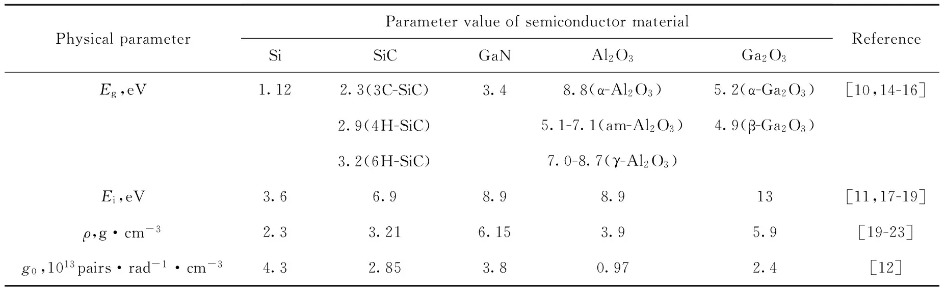
Table 1 Several typical physical characteristic of semiconductor material
1.2 Photocurrent generation of WBGS under pulsed laser
Laser radiation and γ-ray radiation differ significantly in terms of their photon energy. However, in scenarios involving laser radiation, the photoelectric effect becomes the primary mechanism for generating electron-hole pairs, leading to the production of photocurrent. Despite the distinct mechanisms involved, lasers can effectively simulate the dose rate effects observed in WBGS devices. This is attributed to their comparable electrical response and strong correlation with the effects induced by γ-ray irradiation.
The generation of photocurrent in semiconductor materials by laser irradiation involves complex energy transfer mechanisms. When the photon energy of laser exceeds the band gap of the material, there are primarily two absorption mechanisms depending on the number of photons absorbed per electron-hole pair generated: linear absorption and nonlinear absorption. The intensity of the laser at a penetration depthz(cm) within the material, denoted asI(W·cm-2), can be expressed as follows:
(5)
whereI0is the incident light intensity at the surface of the material (z=0);αis the linear absorption coefficient, cm-1, primarily influenced by intrinsic absorption;βrepresents the nonlinear absorption coefficient, cm·W-1, predominantly affected by two photon absorption (TPA).
Then the carrier generation rateGLwithin the material can be expressed by the following equation:
(6)
wherehνis the photon energy andαiis the intrinsic absorption coefficient (αi≈α).
In practical experiments, it is possible to estimate the contribution of TPA by calculating theβI0/αias indicated in Eq.(5)[24]. Taking GaN as an example, under the irradiation conditions of a laser wavelength of 355 nm,αiis approximately 104cm-1, andβis approximately 10-8cm·W-1. When theI0is 107W·cm-2, the excess carrier generation due to TPA accounts for approximately 0.001% of the carrier generation from one-photon absorption. Therefore, the second term in Eq.(6) can be neglected. The relevant properties of other materials can be found in Table 2, and theGLof GaN can be simplified as:
(7)
For SiC devices, since theβI0/αiof SiC is 0.1, TPA needs to be considered.
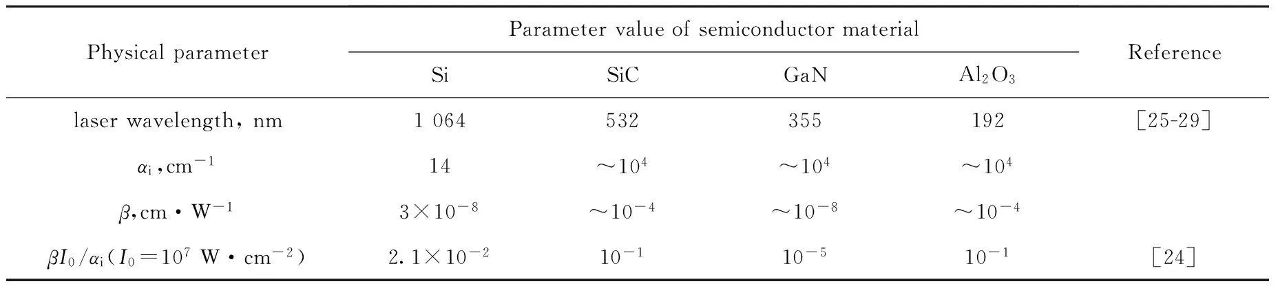
Table 2 Linear and nonlinear absorption coefficient of several semiconductor materials
1.3 Calculation of conversion factor for WBGS
The conversion factor (CF), which is an essential parameter for evaluating the equivalence between laser radiation and γ-ray radiation, plays a significant role in laser-assisted simulation experiments of WBGS devices. Currently, there are three methods available for determining the CF, each based on different reference standards. These methods include the calculation using the carrier generation rate (CGR)[12], peak photocurrent equivalent (PPE)[3], and charge collection equivalent (CCE)[4]. Each of these methods offers a distinct equivalent basis for assessing the similarity between laser radiation and γ-ray radiation.
Take the method of CGR as an example, the calculation method of the CF based on CGR was proposed by Nikiforov et al[12]. According to the mechanisms described in sections 1.1 and 1.2 regarding the effects of γ-ray radiation and laser radiation on WBGS materials, when considering the excess carriers as the equivalent basis, if,
GL=Gγ
(8)
It can be considered that the laser radiation and γ-ray radiation are equivalent in terms of their parameters, and the dose rate corresponding to the laser power density (PL), is referred to as the equivalent dose rate (Peq). And its relation expression is:
Peq=CF·PL
(9)
By combining Eq. (2) and Eq. (7), the average value of CF is given by:
(10)
wherewis the sensitive region thickness, thewvalue of 100 nm, theαivalue of 80 000 cm-1, theβvalue of 7×10⁻⁹cm·W-1, and thehνvalue of 5.6×10⁻¹⁹J, the calculated CF for GaN is approximately 2.59×10⁹rad(Si)·s-1/(W·cm-2) according to the above equation.
The methods of PPE and CCE are different from the theoretical methods of CGR, they all rely on actual γ-ray experimental data. The PPE method will be detailed introduction in the results and analysis section.
2 Device description and experimental setup
2.1 Device description
The GaN-based and SiC-based PIN diodes are both encased in metal packaging with three pins representing the cathode, anode, and grounding (connected to the shell). In order to assess their performance under transient γ-ray radiation and pulsed laser radiation, it is necessary to remove the packaging and expose the internal components of the devices. The unpacked device layouts, which are observed under a microscope, are shown in Fig.1.
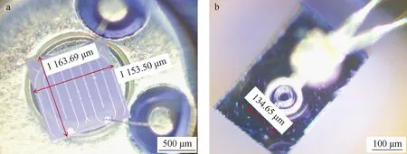
a—GaN-based PIN;b—SiC-based PINFig.1 Layout image of WBGS device
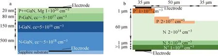
a—GaN-based PIN;b—SiC-based PINFig.2 Structure diagram of GaN-based and SiC-based PIN diodes
The active area of the GaN-based device (W1) is a square with a side length of 1 150 μm, whereas the active area of the SiC-based device (W2) is circular with a diameter of 135 μm. Both W1 and W2 have an active region depth of at least 100 nm. The specific device structure parameters are illustrated in Fig.2. Taking W1 as an example, the heavily doped top layer combines with a metal electrode to form a P-type ohmic contact. The P-GaN region is combined with N-GaN to create a PN junction. Additionally, the I-GaN layer serves as a transition region, facilitating charge balance and current flow limitation. For W2, the stepped P-region with doping concentration of 2×1017cm-3is mainly designed for high voltage resistance and breakdown resistance.
For a laser with a wavelength of 355 nm, theαof GaN and SiC are 80 000 cm-1[30]and 225 cm-1[31], respectively. Fig.3 illustrates the relationship between thezof GaN and SiC materials and the normalized optical power density. As thezincreases, the normalized optical power density decreases to 1/e (approximately 0.37). In the case of GaN, thezis approximately 100 nm, while for SiC, it is around 50 μm. Consequently, the laser with a wavelength of 355 nm can effectively meet the requirements for W1 and W2.
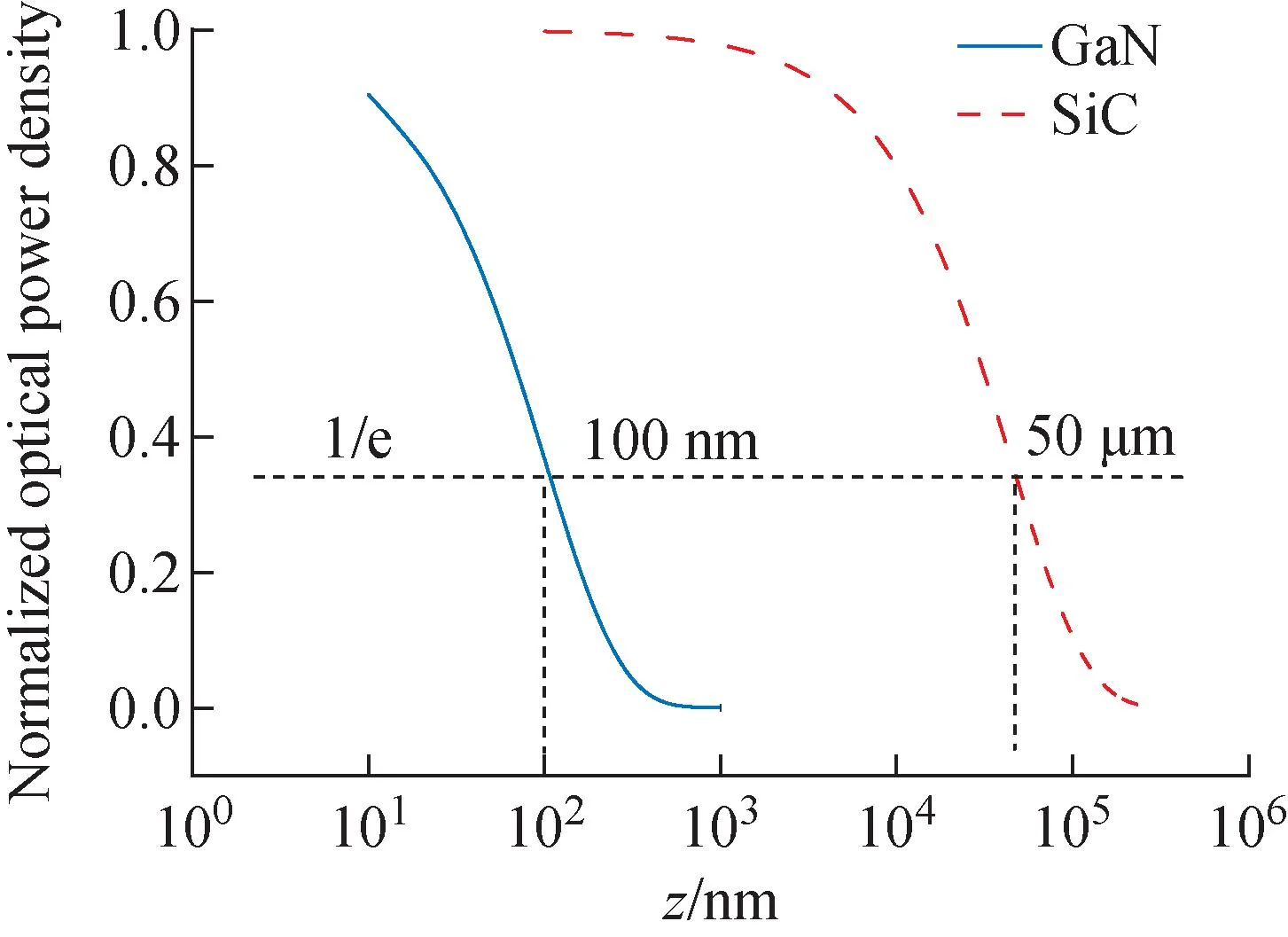
Fig.3 Relationship between penetration depth and normalized optical power density for GaN and SiC
2.2 Experimental setup
The introduction describes the limitations of traditional 532 or 1 064 nm lasers for WBGS materials. These materials, such as GaN, require lasers with shorter wavelengths, specifically around 355 nm, for single-photon ionization absorption. However, this ultraviolet wavelength range is incompatible with the optical lenses, detection, and imaging systems in the original ionizing effect laser-assisted simulation (IELS) system, which operates at 532 or 1 064 nm wavelengths[5]. To address these limitations, the wide band gap ionizing effect laser-assisted simulation (w-IELS) system was designed based on the IELS system[6], as depicted in Fig.4. The w-IELS system operates at a conventional wavelength of 355 nm, with an adjustable wavelength range of 210-2 400 nm. The laser spot can be adjusted using focusing lense or a beam expander, and the laser spot diameter is 3-4 mm to ensure completely and uniformly coverage of the surface of the tested device. The maximum output laser energy of the system is 5.1 mJ with a repetition rate of 1-20 Hz, and a pulse width of 4-7 ns. Furthermore, the stability of the pulse can be controlled within a 5% root mean square (RMS) variation. The system’s optical path includes a short-wavelength pulsed laser passing through an attenuating optical path and being reflected towards a beam-splitter for splitting. A portion of the laser enters a power meter probe to calculate the device’s energy, while the rest, combined with guiding light source, reaches the surface of the semiconductor device under tested. The guiding light source is aligned with the center of the laser spot, facilitating the imaging of the WBGS device test sample using a CCD camera.
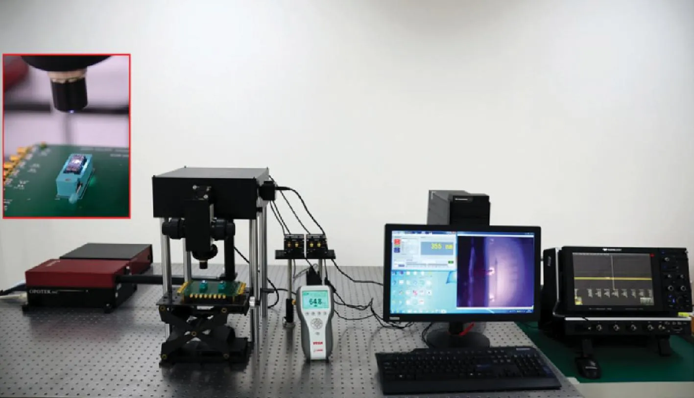
Fig.4 Physical picture of w-IELS system
The dose rate experiments are conducted using the Qiangguang γ-ray generator from the State Key Laboratory of Intense Pulsed Radiation Simulation and Effect of China. The experimental setup is capable of generating γ-ray with a photon energy of 0.9 MeV. The pulse width can be varied within the range of 15-35 ns, and the spot size covers an area of 100 cm2. The dose rate range is from 109to 1011rad(Si)/s. The basic experimental device layout is presented in Fig.5[4].
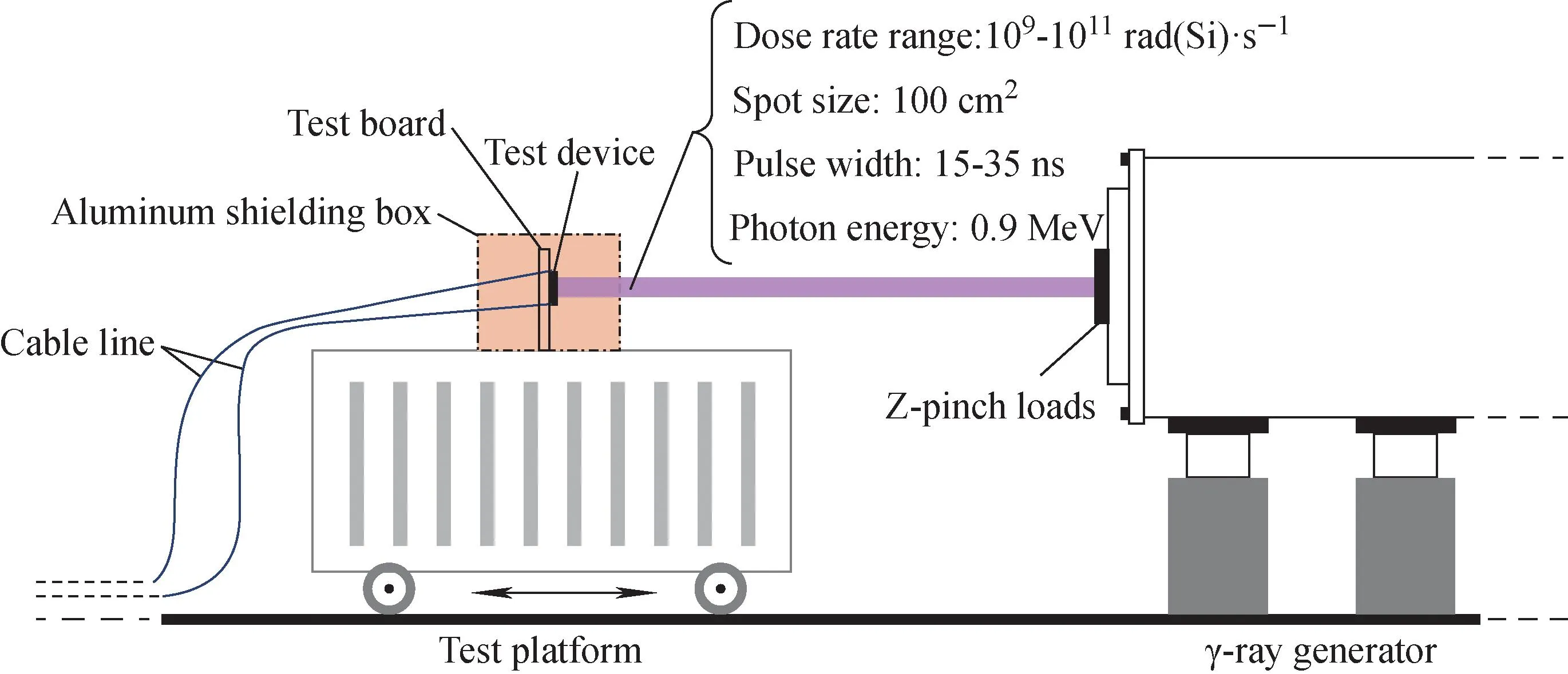
Fig.5 Basic performance parameter of Qiangguang γ-ray generator
In the test circuit, a reverse bias voltage of 5 V and a series resistance of 1 MΩ are chosen. The selection of this resistance is primarily based on the characteristics that WBGS materials require a higher mean ionization energy compared to silicon-based materials, resulting in a lower quantity of excess carriers being generated compared to silicon-based materials at the same dose rate. Consequently, a higher resistance is required to observe an obvious current response in WBGS materials. The GaN-based and SiC-based PIN diodes used in the experiment are small in size and have thin thicknesses. This leads to a weak electrical response generated at the dose rate, which can be easily overshadowed by noise. Taking these factors into consideration, a series resistance of 1 MΩ is determined to ensure an adequate current response. Before conducting the irradiation experiment, theI-Vcurves of the devices are tested, as shown in Fig.6. The leakage currents of GaN-based and SiC-based PIN diodes are below the nA level, which made it convenient to measure the instantaneous current during the device irradiation under the reverse bias voltage of 5 V.
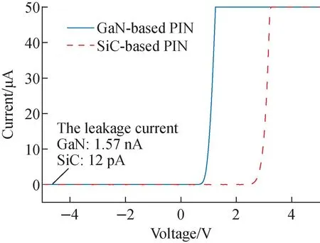
Fig.6 I-V curve of GaN-based and SiC-based PIN diodes
3 Results and analysis
To establish the relationship between the photocurrent and two types of radiation (laser and γ-ray), a series of experiments are conducted. These tests involved measuring the peaks of response (Ipp) under varying laser intensities using the w-IELS system, as well as diverse γ-ray dose rates using the Qiangguang γ-ray generator. The photocurrent response curves of the GaN-based PIN under laser irradiation and γ-ray irradiation are depicted in Fig.7 and Fig.8.
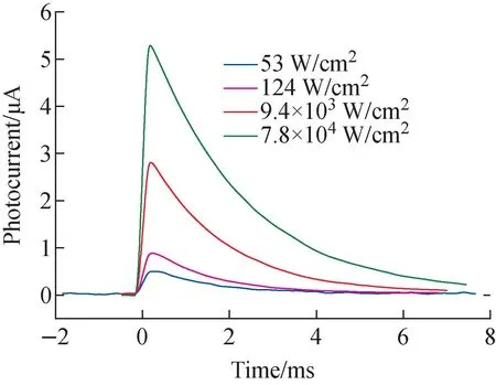
Fig.7 Photocurrent response curve of GaN-based PIN under laser irradiation
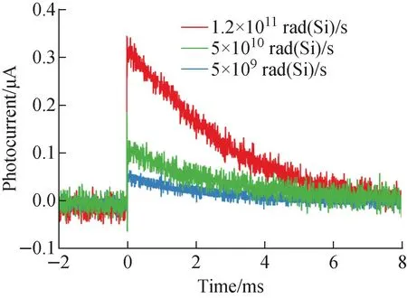
Fig.8 Photocurrent response curve of GaN-based PIN under γ-ray irradiation
Given the maximum dose rate of Qiangguang γ-ray generator is approximately 1×10¹¹rad(Si)/s, the photocurrent peak remains below the μA level. Especially for GaN-based PIN, the photocurrents are even lower than 0.5 μA as shown in Fig.8. In contrast, laser irradiation has the capability to simulate a much wider range of photocurrent response. Due to the need for matching of photocurrent peaks, the irradiation intensity range of both laser radiation and γ-ray radiation is selected based on the range of photocurrent generated by γ-ray radiation.
The calculation method of the CF based on the PPE method establishes a direct relationship between experimental and theoretical aspects. This method utilizes the peak photocurrent generated by both laser radiation and γ-ray radiation devices as the equivalence criterion. To determine the CF, it is essential to extract theIppvalue from the current curves obtained for each intensity level of the laser and γ-ray irradiated devices. The optimization technique is employed to solve for the CF, utilizing log-linear fitting and incorporating the specific relation ofIppversus laser intensity andIppversus dose rate[6]. The expression for the optimized CF is as follows:
(11)
whereF(Ipp) is the fitting function relating the laser power density to the peak photocurrent, andG(Ipp) is the fitting function relating the γ-ray radiation dose rate to the peak photocurrent. CFiis a series of values within a predetermined range, and the optimal CF can be determined through calculation by Eq. (11). As shown in Fig.9, CF1, CF2and CF3are three suitable CFs, and CF2has the best fitting effect. So the CF for W1 is 4.5×10⁸rad(Si)·s-1/(W·cm-2). In comparison to the computed value using the CGR method, which is 2.59×10⁹rad(Si)·s-1/(W·cm-2), the value obtained by PPE is smaller. This is because, in practical experiments, most devices incorporate metal layers (electrodes) that obstruct a portion of incident light from entering the device and generating excess carriers. Additionally, as the laser wavelength increases, thezdecreases, leading to energy dissipation before reaching the active region. The CGR method is difficult to account for these factors, so the CF is mainly calculated through PPE method in this study. Similarly, applying the Eq. (11) to W2 yields a CF of 9×10⁷rad(Si)·s-1/(W·cm-2).
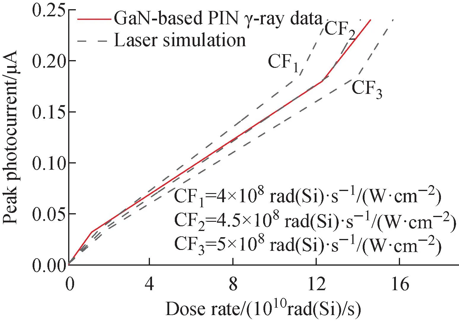
Fig.9 Calculation process of GaN-based PIN equivalent coefficient
Once the CF is obtained, it enables the simulation of a larger range of dose rates based on the results of laser irradiation and the CF. The specific laser-assisted simulation process involves testing the relationship betweenIppversus laser intensity using the w-IELS system, and then obtaining the equivalent dose rate from the product of laser intensity and CF, as described in Eq. (9). Fig.10 presents the results of laser-assisted simulation for GaN-based and SiC-based PIN devices. The data points with error bars represent the experimental values of GaN-based and SiC-based PIN dose rates, while the points without error bars represent the calculated values. The highest dose rate achievable by the Qiangguang γ-ray generator limits the extent of the simulation. To address the problem, a finite-element method (FEM) is adopted in the numerical calculation to supplement high dose rate data, and the software platform is COMSOL Multiphysics 5.5. Additionally, the lines in Fig.10 represent the simulation results obtained from laser radiation on GaN-based and SiC-based PIN devices. It is evident that the relationship between the peak photocurrent and the dose rate is consistent with the relationship between the peak photocurrent and the equivalent dose rate. At dose rates exceeding 1011rad(Si)/s, the laser-assisted simulation technique continues to demonstrate favorable performance. This shows that laser-assisted simulation can better simulate the peak photocurrent characteristic of WBGS devices. At the same time, due to the large adjustment range of laser intensity, the peak photocurrents of WBGS devices at high dose rates could be obtained without the help of FEM numerical simulation.
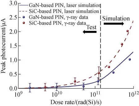
Fig.10 Laser-assisted simulation result of GaN-based and SiC-based PIN devices
To further validate the accuracy of laser-assisted simulation, a dose rate of 1.2×10¹¹rad(Si)/s is selected to compare the actual photocurrent curves of WBGS PIN devices under laser radiation and γ-ray radiation, as shown in Fig.11. The photocurrent responses generated by the laser and γ-ray in GaN-based and SiC-based PIN devices are very similar, and the correlation coefficients are 0.98 and 0.974, respectively. This further confirms that laser-assisted simulation technology is applicable to WBGS devices. As mentioned earlier, due to the influence of the absorption coefficient, short-wavelength lasers in GaN-based devices can only penetrate about 100 nm below the surface. Therefore, for GaN-based light-emitting diodes, laser diodes, and other multilayer devices with thick P-type layers and barrier layers, effectively applying laser-assisted simulation technology remains an urgent problem to be solved.
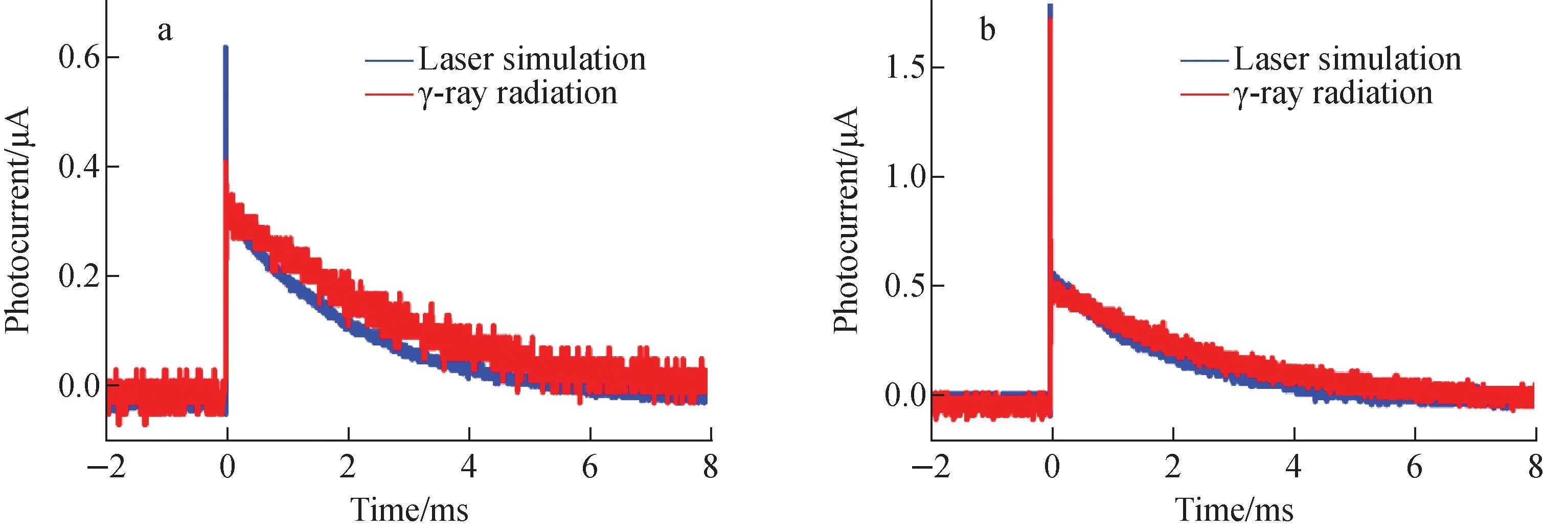
a—GaN-based PIN;b—SiC-based PINFig.11 Response curve of WBGS PIN devices under laser radiation and γ-ray radiation
4 Conclusion
In this paper, the feasibility of laser-assisted simulation of the dose rate effects of WBGS devices is investigated. We have examined the peak photocurrent of WBGS devices under various laser intensities and γ-ray dose rates. By calculating the CF based on the relationship between the photocurrents induced by these two types of radiation, it becomes possible to use laser-assisted simulation to model the dose rate effects of WBGS devices. The results show that laser-assisted simulation is capable of more accurately simulating the peak photocurrent characteristic of WBGS devices, particularly at high dose rate. Moreover, the photocurrent responses of GaN-based and SiC-based PIN diodes under dose rate radiation can be simulated accurately by laser-assisted simulation, and the experimental results of the two are in good agreement.
Acknowledgements:The authors would like to thank Li Qian and Kang Jianbin from the Microsystem &Terahertz Research Center of CAEP, Chengdu, China, for their technical support; Wang Chenhui and Li Ruibin from the State Key Laboratory of Intense Pulsed Radiation Simulation and Effect, Xi’an, China, for their help during the γ-ray radiation experiments.